405.1200.037.2 - Rel.: 2.21 of 25/02/2008
1-3
ated by connection cables or by electronic transmission, it is much more
difficult to suppress it at the inputs of the devices in dangerous areas than at
source,
If possible, disturbance should be suppressed at source.
Disturbance
suppression
circuit - RC
and DIODE
In the following tables there are the specifications of the disturbance sup-
pression filter ciruits.
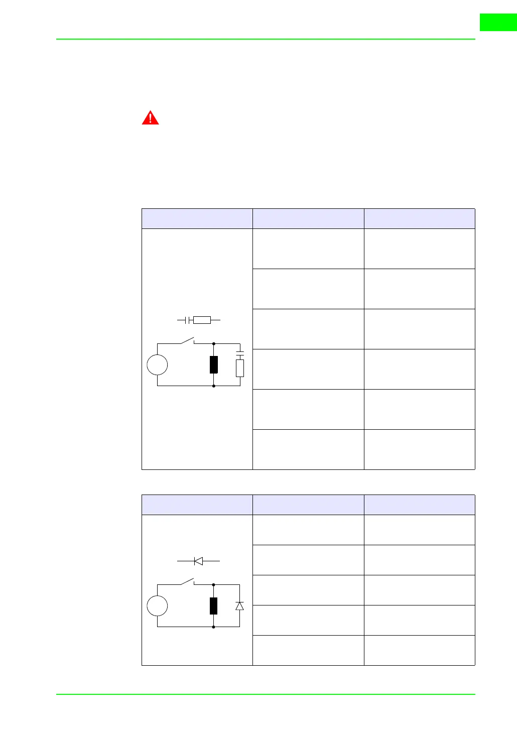
Table 1.1: Disturbance suppression circuit RC
Circuit Advantages Disadvantages
The residual component has a very low
harmonic wave form component.
The best results are obtained by sizing
the R/C suitably.
The residual overvoltage can be limited
to the very low values by optimizing the
sizing.
Volume directly proportional to the
inductance and power of the load.
Switch-off time delay very low.
Optimal suppression is obtained as a
direct consequence of a significant
de-energizing delay.
The effectiveness of the disturbance
suppression is not affected by the volt-
age value. No switch-on delay.
The presence of the capacitor causes a
high load current peak when switching
on (and can cause pasting of the con-
tact if undersized).
Suitable for both AC and DC; no prob-
lem with reversed polarity.
The RC circuit constitutes an additional
load when used with AC.
No arc (low energy) on switching con-
tact.
--
Table 1.2: Disturbance suppression circuit DIODE
Circuit Advantages Disadvantages
Very compact. High switch-off delay time.
No residual voltage (total damping of
disturbance impulse).
For direct current (DC) applications
only.
Easy to size. Polarity must be respected.
--
Switch-off delay can lead to the forma-
tion of a strong electric arc.
--
Sensitive to disturbance voltage pulses
in power supply circuit.
C
Ub
S
L
C
R
Ub
S
LD
D