SO-DIMM Module — Unbuffered SDRAM/SGRAM Graphics
10
Revision 0.91
Module should follow the AC timings specified in the “PC SGRAM” specification.
The graphic controller must assume that the memory is SDRAM unless it can determine that
SGRAM functions (block write and write-per-bit) are available. This can be done at power-up
using the DSF pin. Modules which do not support SGRAM special functions must disable the DSF
pin.
The graphic device must determine the data width of the module, number of row addresses, and
number of column addresses.
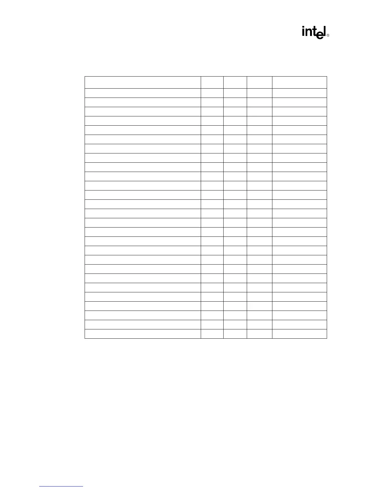
Table 4. Module Baseline Component Requirements
Parameter Min. Max. Unit Notes
Clock Period 15.0 nS
Clock High Time 5.0 nS Rated @ 1.4V
Clock Low Time 5.0 nS
DQM#/CS# Input Setup Time 3.0 nS
Other Input Setup Time 3.0 nS
DQM#/CS# Input Hold Time 1.0 nS
Other Input Hold Time 1.0 nS
Output Valid from Clock 11.0 nS Rated @ 30pf
Output Hold from Clock 2.5 nS Rated @ 30pf
CAS Latency 2 2 Tclk
CAS to CAS Delay 1 Tclk
CAS Bank Delay 1 Tclk
CKE to Clock Disable 1 1 Tclk
RAS Precharge Time 3 Tclk
RAS Active Time 4 Tclk
Activate to Command Delay (RAS to CAS Delay) 2 Tclk
RAS to RAS Bank Activate Delay 2 Tclk
RAS Cycle Time 7 Tclk
DQM to Input Data Delay 0 0 Tclk
Write Cmd. to Input Data Delay 0 0 Tclk
Mode Register set to Active delay 3 Tclk
Precharge to O/P in High-Z 2 Tclk
DQM to Data in HiZ for read 2 2 Tclk
Data in to Precharge 2 Tclk
Data in to Activate/Refresh 5 Tclk
DQM to Data mask for write 0 0 Tclk
Number of Banks per SDRAM/SGRAM device 2 2 Banks