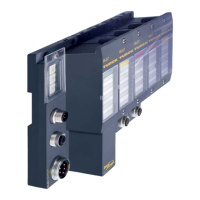
Technology modules
D300529 0115 - BL67 I/O modules12-34
REL_CMP1 0 A comparison of the register contents has produced the
following result:
(REG_SSI_POS) < (REG_CMP1)
1 A comparison of the register contents has produced the
following result:
(REG_ SSI_POS) ≥ (REG_CMP1)
FLAG_CMP1 0 Default status, i.e. the register contents have not yet
matched (REG_SSI_POS) = (REG_CMP1) since the last reset.
1 The contents of the registers match (REG_SSI_POS) =
(REG_CMP1). This marker must be reset with CLR_CMP1 =
1 in the process output data.
STS_CMP1 0 A comparison of the register contents has produced the
following result:
(REG_SSI_POS) ≠ (REG_CMP1)
1 A comparison of the register contents has produced the
following result:
(REG_ SSI_POS) = (REG_CMP1)
REG_WR_ACEPT 0 Writing the user data from the process output to the regis-
ter addressed with REG_WR_ADR in the process output
could not be done.
1 Writing the user data from the process output to the regis-
ter addressed with REG_WR_ADR in the process output
was successful.
REG_WR_AKN 0 No modification of the data in the register bank by process
output, i.e. REG_WR = 0.
A write job would be accepted with the next telegram of
process output data.
(handshake for data transmission to the register.)
1 A modification of the register contents by a process output
was initiated, i.e. REG_WR = 1 → chapter "Process output
(PZDA)".
A write job would not be accepted with the next telegram
of process output data.
Table 12-1:
Meaning of the
data bits (process
input)
Designation Value Description

 Loading...