68
4DL CA 2.4.
The following test procedures can be used for the MT8821C only.
Connection Diagram 2.4.1.
2.4.1.1. Connection Diagram for MT8821C 4DL/1UL CA
2.4.1.1.1. Connection using Main Connector
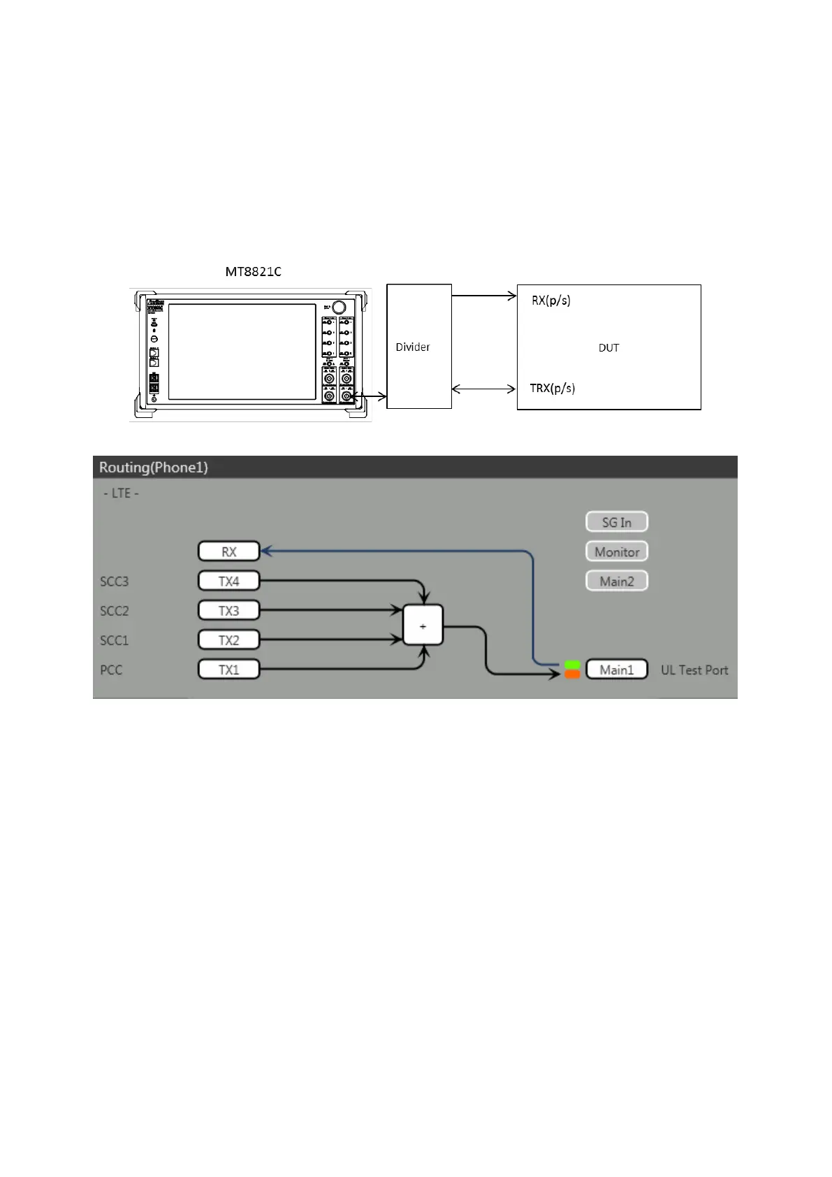
This example shows the connection diagram for 4DL/1UL CA. The DL signals of PCC, SCC1 SCC2 and SCC3 are
combined by the internal combiners of MT8821C and output at Main1 connector of Phone1.
<Connection Diagram>
<Internal Routing Diagram>
Figure 2.4.1-1 Connection Diagram and Internal Routing Diagram for 4DL /UL CA, Tx and Rx Test
(MT8821C, using divider)
[Routing setting procedure]
1. Execute TXOUT 1, MAIN to set the output connector System Config – Routing(Phone1) – Tx1 to Main.
2. Execute TXOUT 2, MAIN to set the output connector System Config – Routing(Phone1) – Tx2 to Main.
3. Execute TXOUT 3, MAIN to set the output connector System Config – Routing(Phone1) – Tx3 to Main.
4. Execute TXOUT 4, MAIN to set the output connector System Config – Routing(Phone1) – Tx4 to Main.