MPC5200B Users Guide, Rev. 1
5-16 Freescale Semiconductor
CDM Registers
5.5.6 CDM Clock Enable Register—MBAR + 0x0214
The CDM Clock Enable Register, or power management register, contains control bits that enable/disable peripheral clocks. Unused
peripherals can have their clock stopped, reducing power consumption.
Bit Name Description
0–4 — Reserved for future use. Write 0.
5 ext_usb_sync_en Enable the synchronization logic which synchronize the external ext_usb_48Mhz
clock to the internal clock system.
bit=1:ext USB 48MHz clock is synchronized to the internal clock system.
bit=0:ext USB 48MHz clock is not synchronized to the internal clock system.
6 ext_usb_48MHz_en USB External 48MHz Clock Select
bit=1:USB 48MHz clock tree sourced from external clock from GPIO.
bit=0:USB 48MHz clock tree sourced from CDM Fractional Divider.
7 ext_irda_48MHz_en IrDA (PSC6) External 48MHz Clock Select
bit=1:IRDA 48MHz clock tree sourced from external clock from GPIO.
bit=0:IRDA 48MHz clock tree sourced from CDM Fractional Divider.
8–14 — Reserved for future use. Write 0.
15 fd_en CDM 48MHz Fractional Divider Enable
bit=1:enable CDM Fractional Divider.
bit=0:disable CDM Fractional Divider.
16 — These fields hold 4 phase divide ratios used by the fractional divider. The fields are
incompletely decoded; f
system
/11 is obtained with 3 values.
110–fractional counter divide ratio f
system
/6
111–fractional counter divide ratio f
system
/7
000–fractional counter divide ratio f
system
/8
001–fractional counter divide ratio f
system
/9
010–fractional counter divide ratio f
system
/10
011–fractional counter divide ratio f
system
/11
10X–fractional counter divide ratio f
system
/11
17–19 cgfd_p3_cnt[2:0]
20 —
21–23 cgfd_p2_cnt[2:0]
24 —
25–27 cgfd_p1_cnt[2:0]
28 —
29–31 cgfd_p0_cnt[2:0]
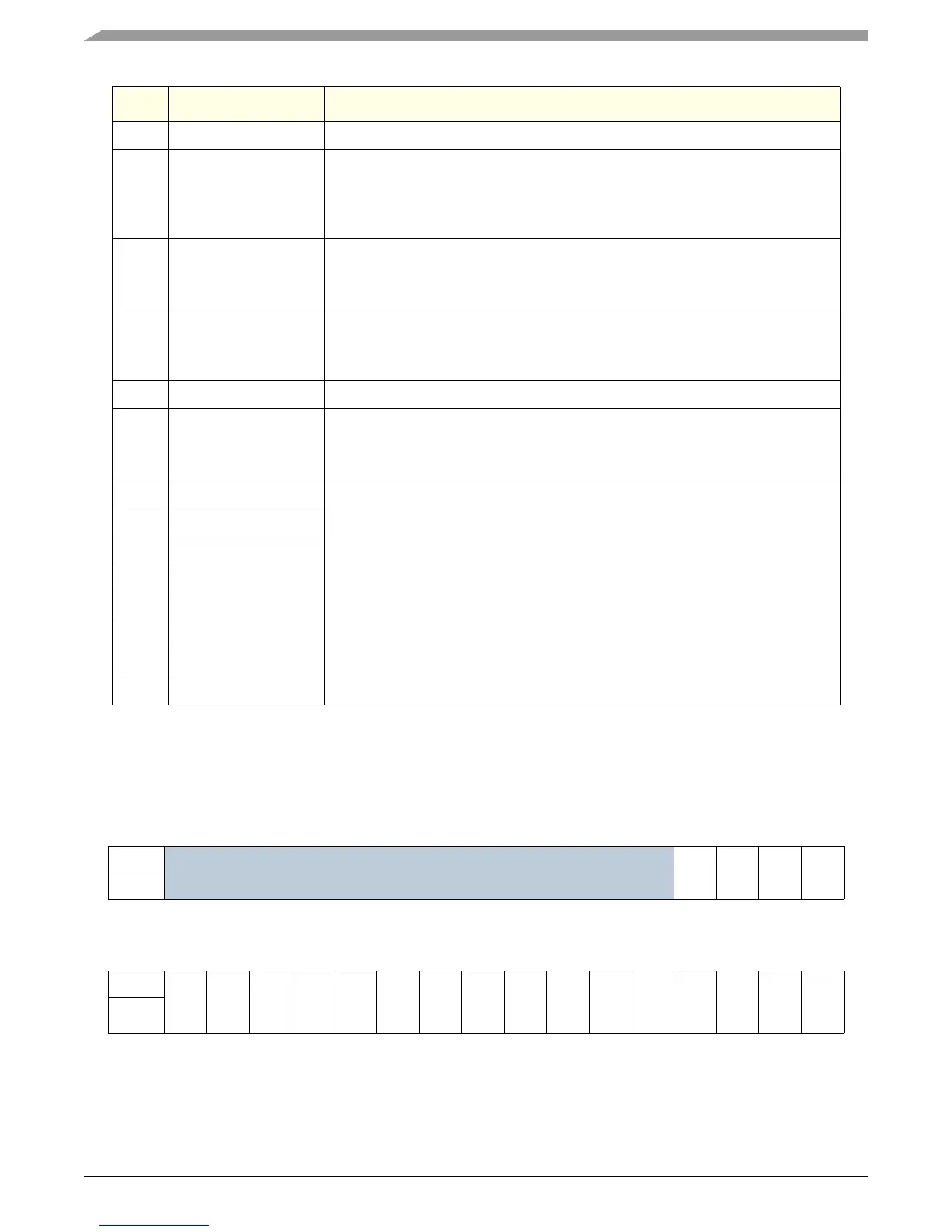
Table 5-13. CDM Clock Enable Register
msb 0123456789101112131415
R
Reserved
Write 0
mem_
clk_en
pci_
clk_en
lpc_
clk_en
slt_
clk_en
W
RESET: 0 0 0 0000011111111
16 17 18 19 20 21 22 23 24 25 26 27 28 29 30 31 lsb
R
scom_
clk_en
ata_
clk_en
eth_
clk_en
usb_
clk_en
spi_
clk_en
bdlc_clk_
en
psc5_
clk_en
psc4_
clk_en
psc3_
clk_en
psc2_
clk_en
psc1_
clk_en
psc6
clk_en
mscan_
clk_en
i2c_
clk_en
timer_
clk_en
gpio_
clk_en
W
RESET: 1 1 1 1111111111111