MPC5200B Users Guide, Rev. 1
11-4 Freescale Semiconductor
ATA Register Interface
11.3.1.4 ATA PIO Timing 2 Register—MBAR + 0x3A0C
11.3.1.5 ATA Multiword DMA Timing 1 Register—MBAR + 0x3A10
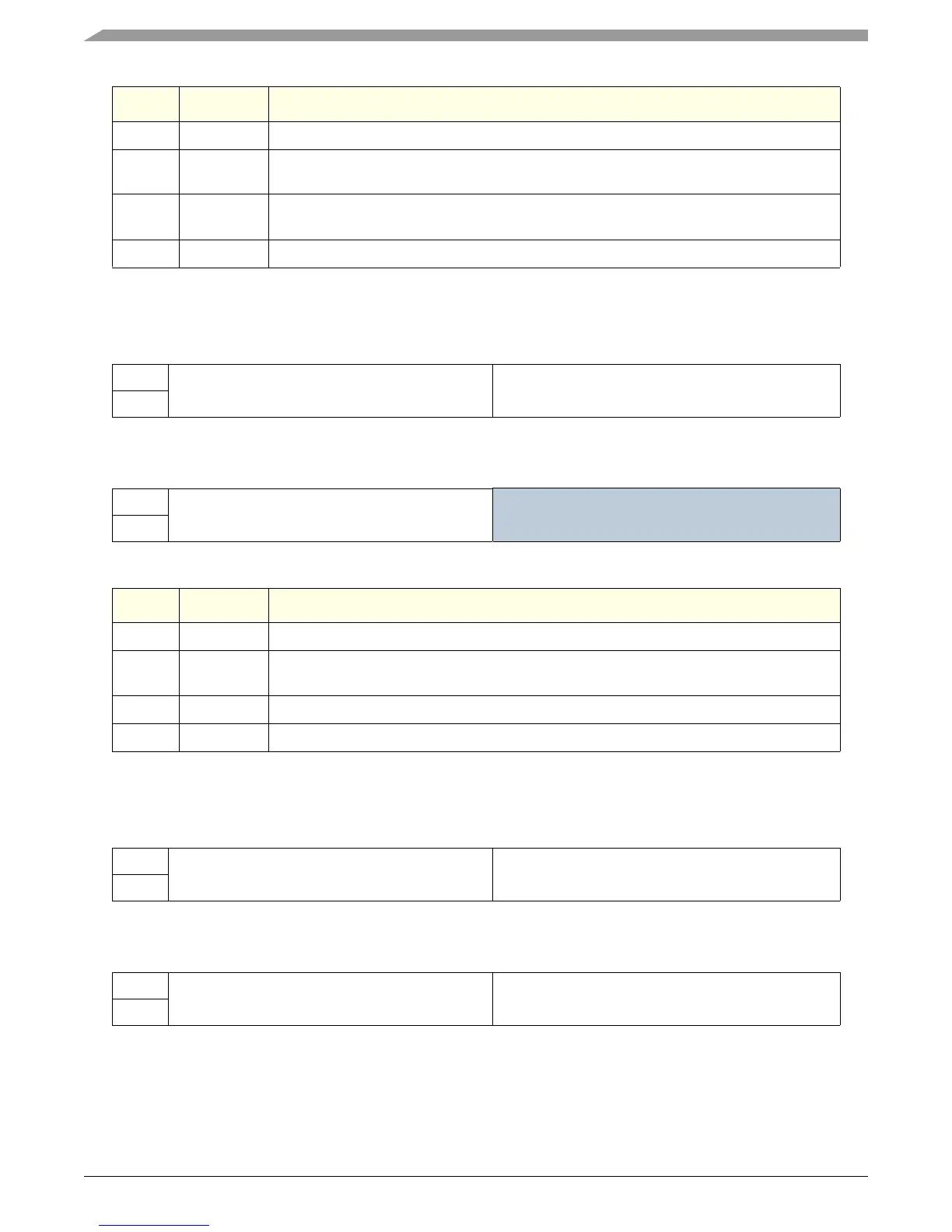
Bits Name Description
0:7 pio_t0 PIO cycle time count value is based on system clock operating frequency.
8:15 pio_t2_8 PIO read/write pulse width for 8-bit transfers. Count value is based on system clock
operating frequency.
16:23 pio_t2_16 PIO read/write pulse width for 16-bit transfers. Count value is based on system clock
operating frequency.
24:31 — Reserved
Table 11-4. ATA PIO Timing 2 Register
msb 012345678 9 1011121314 15
R pio_t4 pio_t1
W
RESET:0 00000000 0 0 0 00 0 0
16 17 18 19 20 21 22 23 24 25 26 27 28 29 30 31 lsb
R pio_ta
Reserved
W
RESET:0 00000000 0 0 0 00 0 0
Bits Name Description
0:7 pio_t4 PIO write (DIOW) data hold time. Count value is based on system clock operating frequency.
8:15 pio_t1 Address valid to DIOR/DIOW setup. Count value is based on system clock operating
frequency.
16:23 pio_ta IORDY setup time. Count value is based on system clock operating frequency.
24:31 — Reserved
Table 11-5. ATA Multiword DMA Timing 1 Register
msb 012345678 9 1011121314 15
R dma_t0 dma_td
W
RESET:0 00000000 0 0 0 00 0 0
16 17 18 19 20 21 22 23 24 25 26 27 28 29 30 31 lsb
R dma_tk dma_tm
W
RESET:0 00000000 0 0 0 00 0 0