MPC5200B Users Guide, Rev. 1
17-4 Freescale Semiconductor
SPI Registers—MBAR + 0x0F00
17.3.2 SPI Control Register 2—MBAR + 0x0F01
6 SSOE Slave Select (SS) Output Enable—bit is enabled only in master mode by asserting SSOE and
SPIDDR bit 3 as shown in Table 17-3.
7 LSBFE SPI LSB-First Enable—bit does not affect the position of the msb and lsb in the data register.
Reads and writes of the data register always have the msb in bit 7.
0 = Data is transferred most significant bit first.
1 = Data is transferred least significant bit first.
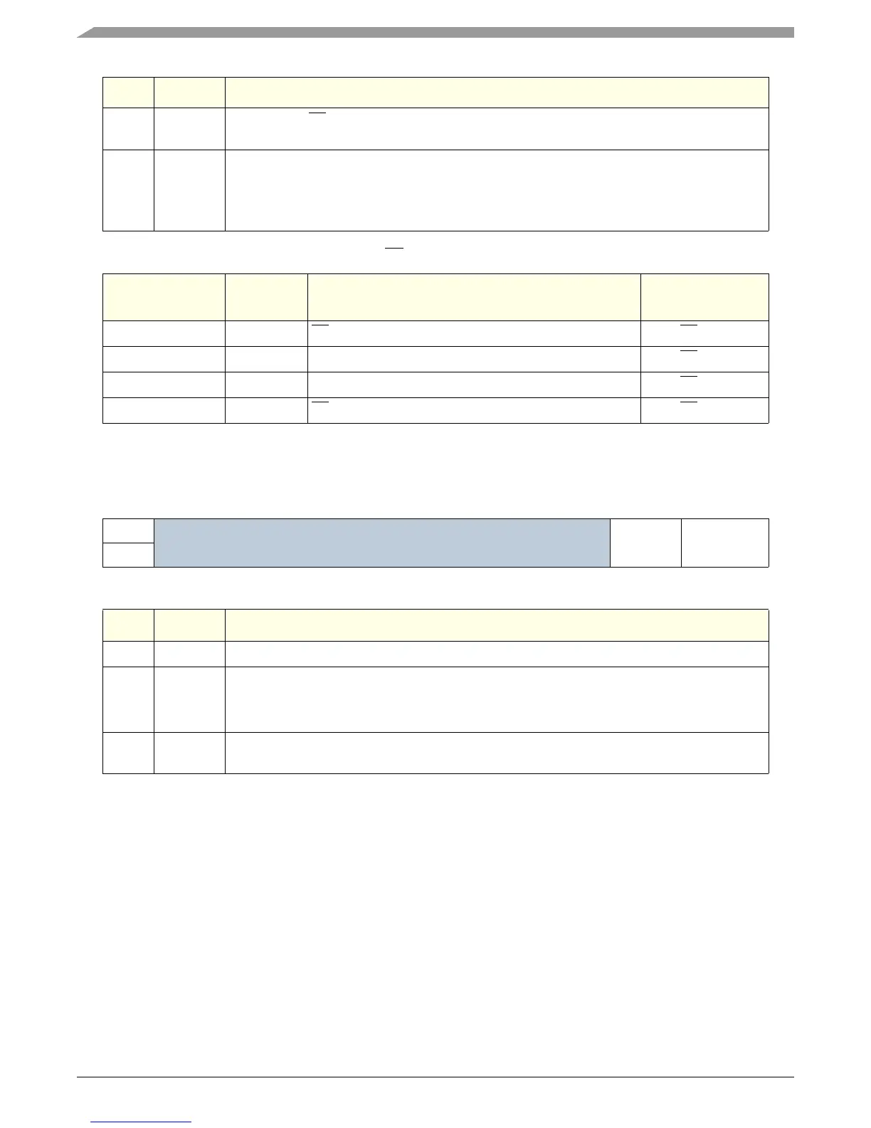
Table 17-3. SS Input/Output Selection
SPIDDR Bit 4
(DDR3)
SSOE Master Mode Slave Mode
00SS
input with MODF feature SS input
0 1 General-purpose input SS input
1 0 General-purpose output SS input
11SS output SS input
Table 17-4. SPI Control Register 2
msb 0 1 2 3 4 5 6 7 lsb
R
Reserved SPISWAI SPC0
W
RESET:00000000
Bit Name Description
0:5 — Reserved
6 SPISWAI SPI Stop in Wait Mode—bit is used for power conservation while in wait mode.
0 = SPI clock operates normally in wait mode
1 = Stop SPI clock generation when in wait mode
7 SPC0 Serial Pin Control Bit 0—working with the MSTR control bit, this bit enables bidirectional pin
configurations as shown in Ta ble 1 7- 5.
Bit Name Description