MPC5200B Users Guide, Rev. 1
8-14 Freescale Semiconductor
Features
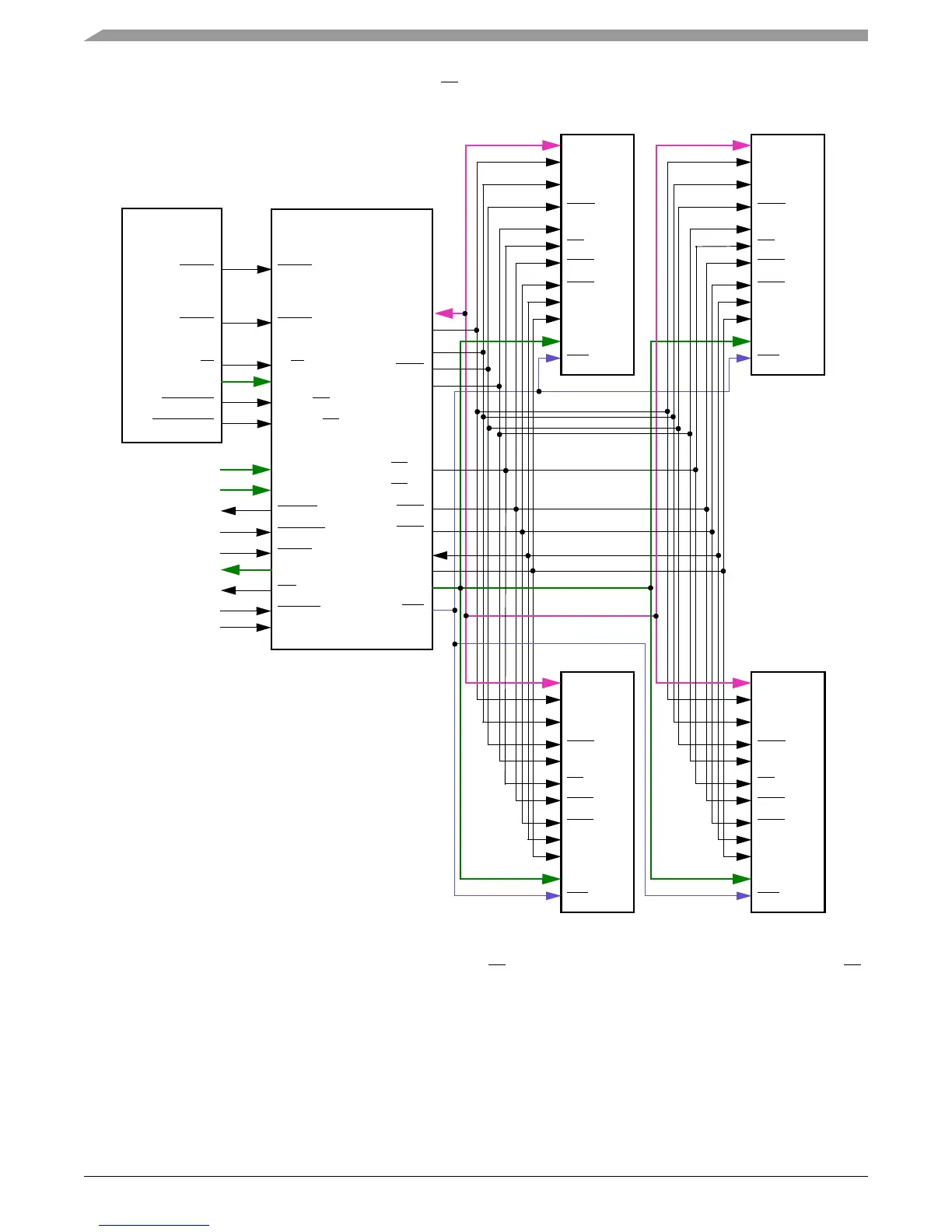
Figure 8-1 shows an example memory configuration of 1 space (CS) of 4 devices of 128Mbit (4M x 4 banks x 8bit) DDR SDRAM, for a total
memory size of 64MB.
Figure 8-1. Block Diagram—SDRAM Subsystem Example
Both chip selects contribute together to access the whole memory. Each CS base address and size are programmed independently. Each CS
base address must be size-aligned.
The MPC5200B does not support DIMM memory modules, however it can support a DIMM-compatible EEPROM using an on-chip I
2
C chip
interface (with appropriate configuration of pin functions).
DQ[31:0]
BA[1:0]
CLK
CLK
CKE
CS
[0]
CS[1]
RAS
CAS
DQS[3:0]
DM[3:0]
MA[11:0]
WE
DQ[7:0]
BA[1:0]
CLK
CLK
CKE
CS
RAS
CAS
DQS
DM
A[11:0]
WE
DQ[7:0]
BA[1:0]
CLK
CLK
CKE
CS
RAS
CAS
DQS
DM
A[11:0]
WE
7:0
15:8
A[11:0]
DQ[31:0]
D_CS
R/W
DM_I[0:7]
D_CS
R/W
DM[0:7]
REG_
CS REG_CS
A_CSA_CS
ADDR[4:29]
AACK
ARTRY
TBST
DO[0:63]
TA
processor bus
SDRAMGlue
RESET
CLK
REGD_CSREGD_CS
DI[0:63]
DQ[7:0]
BA[1:0]
CLK
CLK
CKE
CS
RAS
CAS
DQS
DM
A[11:0]
WE
DQ[7:0]
BA[1:0]
CLK
CLK
CKE
CS
RAS
CAS
DQS
DM
A[11:0]
WE
Memory Controller
0
1
2
3
23:16 31:24
0
1
3
2
Note: For 16-Bit External Data Width,
mem_ps = 1, only DQ[31:16] should
be connected to the external memories.