MPC5200B Users Guide, Rev. 1
14-26 Freescale Semiconductor
FEC Registers—MBAR + 0x3000
Note: X: Bit is not reset and must be initialized.
14.5.20 FEC Tx FIFO Watermark Register—MBAR + 0x3144
The X_WMRK register is a user programmable 4-bit read/write register that controls the amount of data required in the transmit FIFO before
transmission of a frame can begin. This lets the user minimize transmit latency (X_WMRK = 0000) or allows for larger bus access latency
(X_WMRK = 1111) due to contention for the system bus. Setting the watermark to a high value minimizes the risk of transmit FIFO underrun
due to contention for the system bus. The X_WMRK register resets to 0.
NOTE
This register value may need to be customized by software for specific FEC applications to be
compatible with specific FIFO/system bus access latency requirements.
16 17 18 19 20 21 22 23 24 25 26 27 28 29 30 31 lsb
R GADDR2
W
RESET:X XXXXXXXX X X X XX X X
Bits Name Description
0:31 GADDR2 The GADDR2 register contains the lower 32bits of the 64-bit hash table used in the address
recognition process for receive frames with a multicast address.
• Bit 31 contains hash index bit 31.
• Bit 0 contains hash index bit 0.
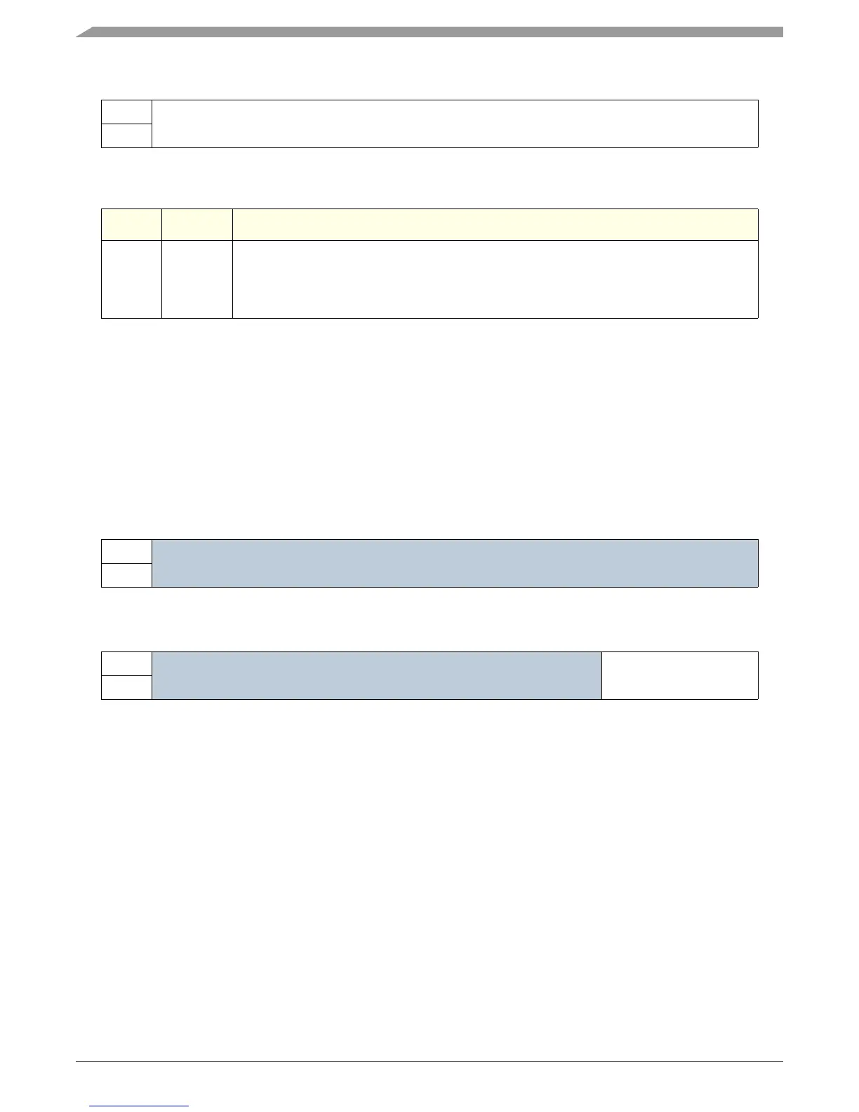
Table 14-29. FEC Tx FIFO Watermark Register
msb 012345678 9 1011121314 15
R
Reserved
W
RESET:0 00000000 0 0 0 00 0 0
16 17 18 19 20 21 22 23 24 25 26 27 28 29 30 31 lsb
R
Reserved X_WMRK
W
RESET:0 00000000 0 0 0 00 0 0