MPC5200B Users Guide, Rev. 1
15-4 Freescale Semiconductor
PSC Registers—MBAR + 0x2000, 0x2200, 0x2400, 0x2600, 0x2800, 0x2C00
• Selectable pulse width: either 3/16 bit duration or 1.6 µs
IrDA MIR mode:
• Baud rate: 0.576 Mbps to 1.152 Mbps
IrDA FIR mode:
• Baud rate: 4 Mbps
15.2 PSC Registers—MBAR + 0x2000, 0x2200, 0x2400, 0x2600, 0x2800, 0x2C00
The PSCs are located at an address as indicated below:
• PSC1 BASE = MBAR + 0x2000
• PSC2 BASE = MBAR + 0x2200
• PSC3 BASE = MBAR + 0x2400
• PSC4 BASE = MBAR + 0x2600
• PSC5 BASE = MBAR + 0x2800
• PSC6 BASE = MBAR + 0x2C00
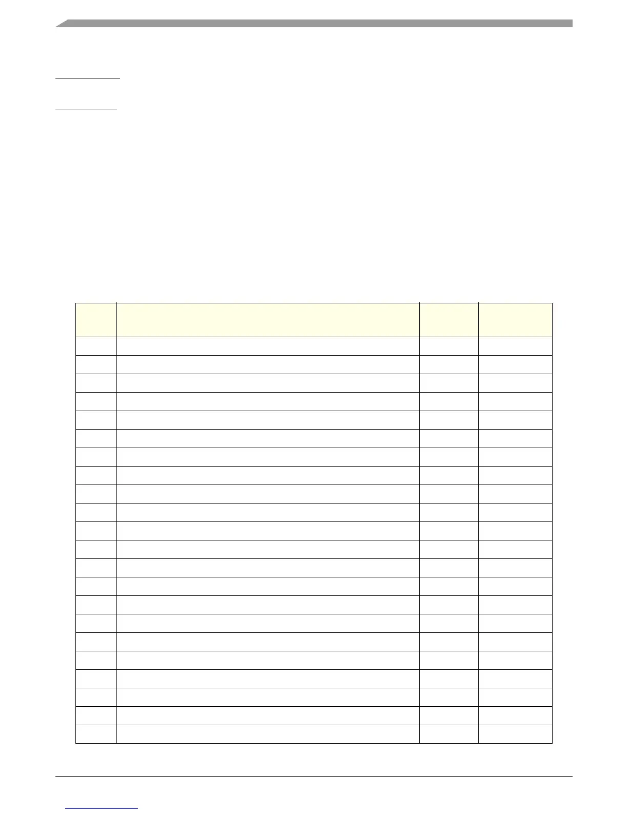
Each PSC uses 42 registers. The register address is calculated as base address for the regarding PSC plus the offset value. Table 15-2 shows
the list with all implemented registers and the associated offset value.
Table 15-2. PSC Memory Map
Offset Register Name
Register
width
Access
00 Mode Register 1 (0x00)—MR1 8R/W
00 Mode Register 2 (0x00) — MR2 8R/W
04 Status Register (0x04) — SR 16 R
04 Clock Select Register (0x04) — CSR 16 W
08 Command Register (0x08)—CR 8R/W
0C Rx Buffer Register (0x0C) — RB 32 R
0C Tx Buffer Register (0x0C)—TB 32 W
10 Input Port Change Register (0x10) — IPCR 8R
10 Auxiliary Control Register (0x10) — ACR 8W
14 Interrupt Status Register (0x14) — ISR 16 R
14 Interrupt Mask Register (0x14)—IMR 16 W
18 Counter Timer Upper Register (0x18)—CTUR 8W
1C Counter Timer Lower Register (0x1C)—CTLR 8W
20 Codec Clock Register (0x20)—CCR 32 R/W
24 AC97 Slots Register (0x24)—AC97Slots 32 W
28 AC97 Command Register (0x28)—AC97CMD 32 R/W
2C AC97 Status Data Register (0x2C)—AC97Data 32 R
30 Interrupt Vector Register (0x30)—IVR - Reserved 8 R/W
34 Input Port Register (0x34)—IP 8R
38 Output Port 1 Bit Set (0x38)—OP1 8W
3C Output Port 0 Bit Set (0x3C)—OP0 8W
40 Serial Interface Control Register (0x40)—SICR 32 R/W