MPC5200B Users Guide, Rev. 1
10-34 Freescale Semiconductor
Registers
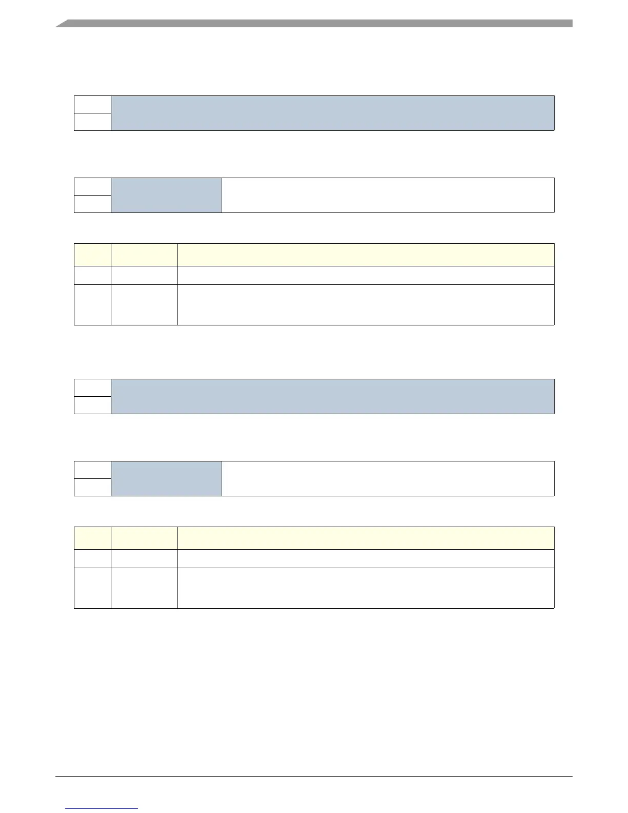
10.3.3.1.14 Tx FIFO Read Pointer Register PCITFRPR(RW) —MBAR + 0x3850
10.3.3.1.15 Tx FIFO Write Pointer Register PCITFWPR(RW) —MBAR + 0x3854
This marks the end of the PCI Multi-Channel DMA Transmit Interface description.
10.3.3.2 Multi-Channel DMA Receive Interface
PCI Rx is controlled by 13 32-bit registers. These registers are located at an offset from MBAR. Register addresses are relative to this offset.
msb 012345678 9 1011121314 15
R
Reserved
W
RESET 0 00000000 0 0 0 00 0 0
16 17 18 19 20 21 22 23 24 25 26 27 28 29 30 31 lsb
R
Reserved ReadPtr
W
RESET 0 00000000 0 0 0 00 0 0
Bits Name Description
0:19 Reserved Unused. Software should write zero to these bits.
20:31 ReadPtr This value is maintained by FIFO hardware and is NOT normally written. It can be adjusted
in special cases, but this disrupts data flow integrity. The value represents the Read address
presented to the FIFO RAM.
msb 012345678 9 1011121314 15
R
Reserved
W
RESET 0 00000000 0 0 0 00 0 0
16 17 18 19 20 21 22 23 24 25 26 27 28 29 30 31 lsb
R
Reserved WritePtr
W
RESET 0 00000000 0 0 0 00 0 0
Bits Name Description
0:19 Reserved Unused bits. Software should write zero to these bits.
20:31 WritePtr Value is maintained by FIFO hardware and is NOT normally written. It can be adjusted in
special cases, but this disrupts data flow integrity. Value represents the Write address
presented to the FIFO RAM.
 Loading...