MPC5200B Clock Domains
MPC5200B Users Guide, Rev. 1
Freescale Semiconductor 5-3
5.3.1 MPC5200B Top Level Clock Relations
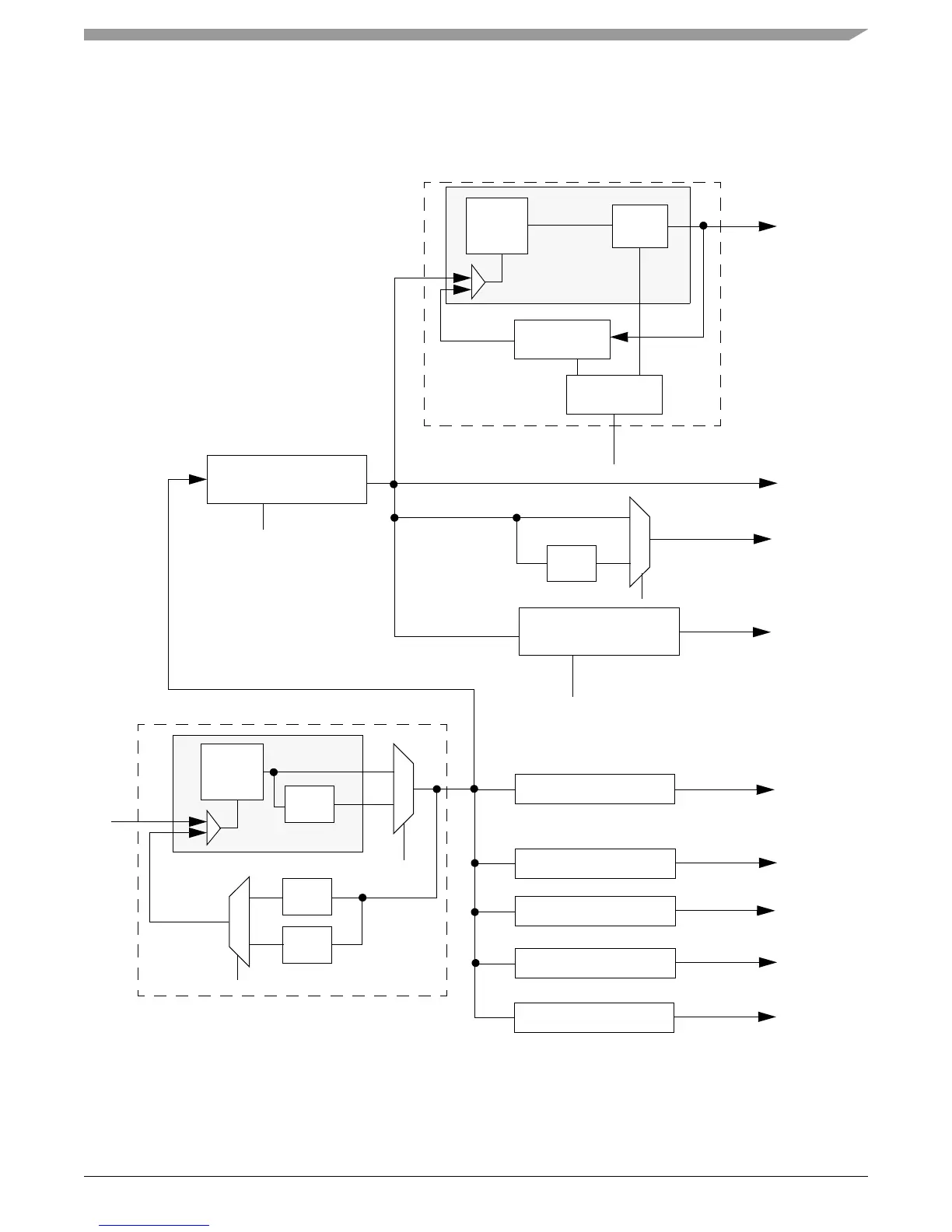
Figure 5-2 shows the CDM clock divide circuitry. This picture shows only the functional clocks. The clock network regarding the scan and
bypass modes is not included.
Figure 5-2. MPC5200 Clock Relations
SYS_XTAL_IN
XLB CLOCK
MEM CLOCK
IPB CLOCK
PSC1 MCLK DIVIDER
f
system
/ (MclkDiv[8:0]+1)
PSC1 MCLK
System APLL
VCO
f
system
divide
by 12
divide
by 16
1
0
sys_pll_cfg[0]
1
0
sys_pll_cfg[1]
f
VCOsys
by 2
divide
Fractional Divider
f
system
/ (6, 6.25, 6.5 ...11)
48 MHz CLOCK
USB CLOCK
PSC2 MCLK DIVIDER
f
system
/ (MclkDiv[8:0]+1)
PSC2 MCLK
PSC3 MCLK DIVIDER
f
system
/ (MclkDiv[8:0]+1)
PSC3 MCLK
PSC6 MCLK DIVIDER
f
system
/ (MclkDiv[8:0]+1)
PSC6 MCLK
e300
VCO
divide by
2, 2.5,3.0 ...7.5, 8
e300
CORE CLOCK
Core APLL
XLB Clock Divider
f
system
/ (8 or 4)
xlb_clk_sel
divide
by 2
0
1
ipb_clk_sel
PCI Clock Divider
xlb_clk_sel
PCI CLOCK
ipb_clk_sel
pci_clk_sel[1:0]
divide by
2 or 4
Core APLL
Control Logic
rst_cfg[0:4]
ppc_pll_cfg[0:4]
f
VCOcore