MPC5200B Users Guide, Rev. 1
10-44 Freescale Semiconductor
Functional Description
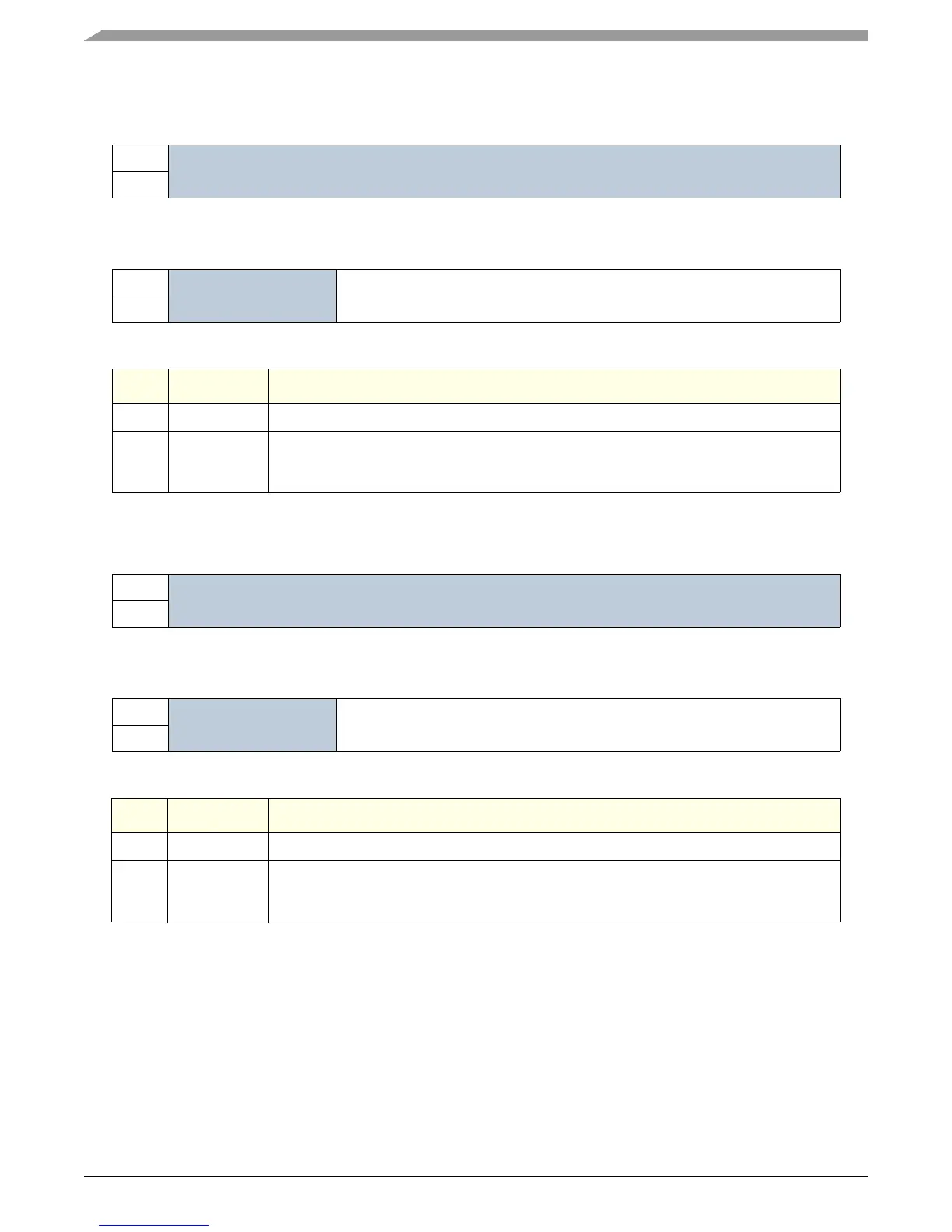
10.3.3.2.14 Rx FIFO Read Pointer Register PCIRFRPR(RW) —MBAR + 0x38D0
10.3.3.2.15 Rx FIFO Write Pointer Register PCIRFWPR (RW) —MBAR + 0x38D4
This marks the end of the PCI Multi-Channel DMA Receive Interface description.
10.4 Functional Description
The MPC5200B PCI module provides both master and target PCI bus interfaces as shown in Figure 10-1. The internal PCI master, or initiator,
interface is accessible by any XL bus master such as the processor core and also provides a DMA interface (for BestComm) through the
Communication Sub-System, which can be accessed by the Multi-Channel DMA engine. The internal PCI target interface provides external
PCI masters access into two memory windows of MPC5200B address space. PCI arbitration is handled external to this module, by the
MPC5200B internal PCI arbiter.
msb 012345678 9 1011121314 15
R
Reserved
W
RESET 0 00000000 0 0 0 00 0 0
16 17 18 19 20 21 22 23 24 25 26 27 28 29 30 31 lsb
R
Reserved ReadPtr
W
RESET 0 00000000 0 0 0 00 0 0
Bits Name Description
0:19 Reserved Unused. Software should write zero to these bits.
20:31 ReadPtr This value is maintained by the FIFO hardware and is not normally written. It can be adjusted
in special cases but will disrupt the integrity of the data flow. This value represents the Read
address being presented to the FIFO RAM.
msb 012345678 9 1011121314 15
R
Reserved
W
RESET 0 00000000 0 0 0 00 0 0
16 17 18 19 20 21 22 23 24 25 26 27 28 29 30 31 lsb
R
Reserved WritePtr
W
RESET 0 00000000 0 0 0 00 0 0
Bits Name Description
12:19 Reserved Unused. Software should write zero to these bits.
20:31 WritePtr This value is maintained by the FIFO hardware and is not normally written. It can be adjusted
in special cases but will of course disrupt the integrity of the data flow. This value represents
the Write address being presented to the FIFO RAM.