I
2
C Interface Registers
MPC5200B Users Guide, Rev. 1
Freescale Semiconductor 18-5
Figure 18-6. Timing Diagram—Clock Synchronization
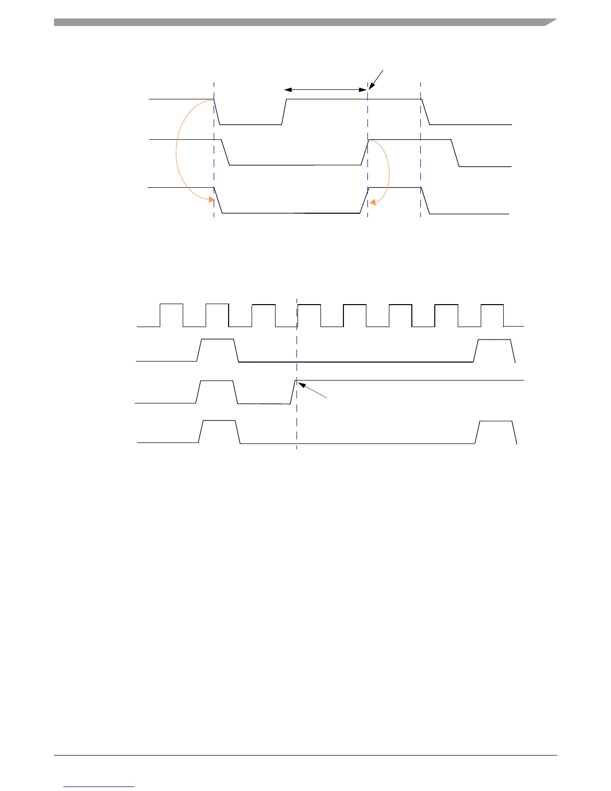
A data arbitration procedure determines the relative priority of contending masters. A bus master loses arbitration if it transmits logic “1”
while another master transmits logic “0”. Losing masters immediately switch to slave-receive mode and stop driving SDA output. In this case,
transition from master to slave mode does not generate a STOP condition. A status bit is hardware set to indicate loss of arbitration. See
Figure 18-7.
Figure 18-7. Timing Diagram—Arbitration Procedure
18.3 I
2
C Interface Registers
The I
2
C is controlled by 7 32-bit registers. The registers are located at an offset from MBAR of 0x3D00 (I2C1) and 0x3D40 (I2C2) . Register
addresses are relative to this offset. There is one I
2
C Interrupt Control Register only for both I
2
C modules. There is also one glitch filter control
register for both I2C modules.
Hyperlinks to the I
2
C Interface registers are provided below:
• I
2
C Address Register (0x3D00) • I
2
C Status Register (0x3D0C)
• I
2
C Frequency Divider Register (0x3D04) • I
2
C Data I/O Register (0x3D10)
• I
2
C Control Register (0x3D08) • I
2
C Interrupt Control Register (0x3D20)
• I
2
C Filter Register (0x3D24) •
Wait State
Start Counting
High Period
SCL by
SCL by
SCL
Master1
Master2
SCL
SDA by
Master1
SDA by
Master2
SDA
Master 2 Loses Arbitration,
and becomes slave-receiver