MPC5200B Users Guide, Rev. 1
9-28 Freescale Semiconductor
Programmer’s Model
9.7.3 SCLPC FIFO Registers—MBAR + 0x3C40
LPC uses a single FIFO that changes direction based on the Rx/Tx mode. Software controls direction change and flushes FIFO before
changing directions. FIFO memory is 512Bytes (32 x 128).
LPC FIFO is controlled by six 32-bit registers. These registers are located at an offset from MBAR of 0x3C40. Register addresses are relative
to this offset. Therefore, the actual register address is: MBAR + 0x3C40 + register address
Hyperlinks to the LPC FIFO registers are provided below:
9.7.3.1 LPC Rx/Tx FIFO Data Word Register—MBAR + 0x3C40
LPC_rx/tx_fifo_data_word_register
Note: X: Bit does not reset to a defined value.
• Section 9-18, LPC Rx/Tx FIFO Data Word Register
(0x3C40)
• Section 9-21, LPC Rx/Tx FIFO Alarm Register
(0x3C4C)
• Section 9-19, LPC Rx/Tx FIFO Status Register
(0x3C44)
• Section 9-22, LPC Rx/Tx FIFO Read Pointer Register
(0x3C50)
• Section 9-20, LPC Rx/Tx FIFO Control Register
(0x3C48)
• Section 9-23, LPC Rx/Tx FIFO Write Pointer Register
(0x3C54)
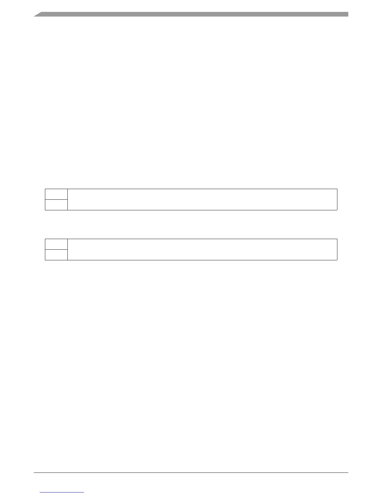
Table 9-18. LPC Rx/Tx FIFO Data Word Register
msb 012345678 9 1011121314 15
R FIFO_Data_Word
W
RESET:X XXXXXXXX X X X XX X X
16 17 18 19 20 21 22 23 24 25 26 27 28 29 30 31 lsb
R FIFO_Data_Word
W
RESET:X XXXXXXXX X X X XX X X