FEC Registers—MBAR + 0x3000
MPC5200B Users Guide, Rev. 1
Freescale Semiconductor 14-17
14.5.7 FEC MII Management Frame Register—MBAR + 0x3040
This MII_DATA register does not reset to a defined value. The MII_DATA register is used to communicate with the attached MII compatible
PHY device(s), providing read/write access to the MII registers.
Writing to the MII_DATA register causes a management frame to be sourced unless the MII_SPEED register has been programmed to 0. When
writing to MII_DATA when MII_SPEED = 0, if the MII_SPEED register is then written to a non-zero value, an MII frame is generated with
the data previously written to the MII_DATA register. This let MII_DATA and MII_SPEED be programmed in either order if MII_SPEED is
currently 0.
Note: X: Bit does not reset to a defined value.
To do a read or write operation the MII management interface writes to the MII_DATA register. To generate a valid read or write management
frame:
• the ST field must be written with a 01
• the OP field must be written with either:
— 01 (management register write frame), or
— 10 (management register read frame), and
• the TA field must be written with a 10
If other patterns are written to these fields, a frame is generated, but it does not comply to the IEEE 802.3 MII definition:
• OP field = 1x produces a “read” frame operation, while
• OP field = 0x produces a “write” frame operation.
To generate an IEEE 802.3 compliant MII management interface write frame (write to a PHY register), the user must write the following to
the MII_DATA register:
{01 01 PHYAD REGAD 10 DATA}
Writing this pattern causes control logic to shift out the data in the MII_DATA register following a preamble generated by the control state
machine. During this time, the MII_DATA register contents are altered as the contents are serially shifted, and is unpredictable if read by the
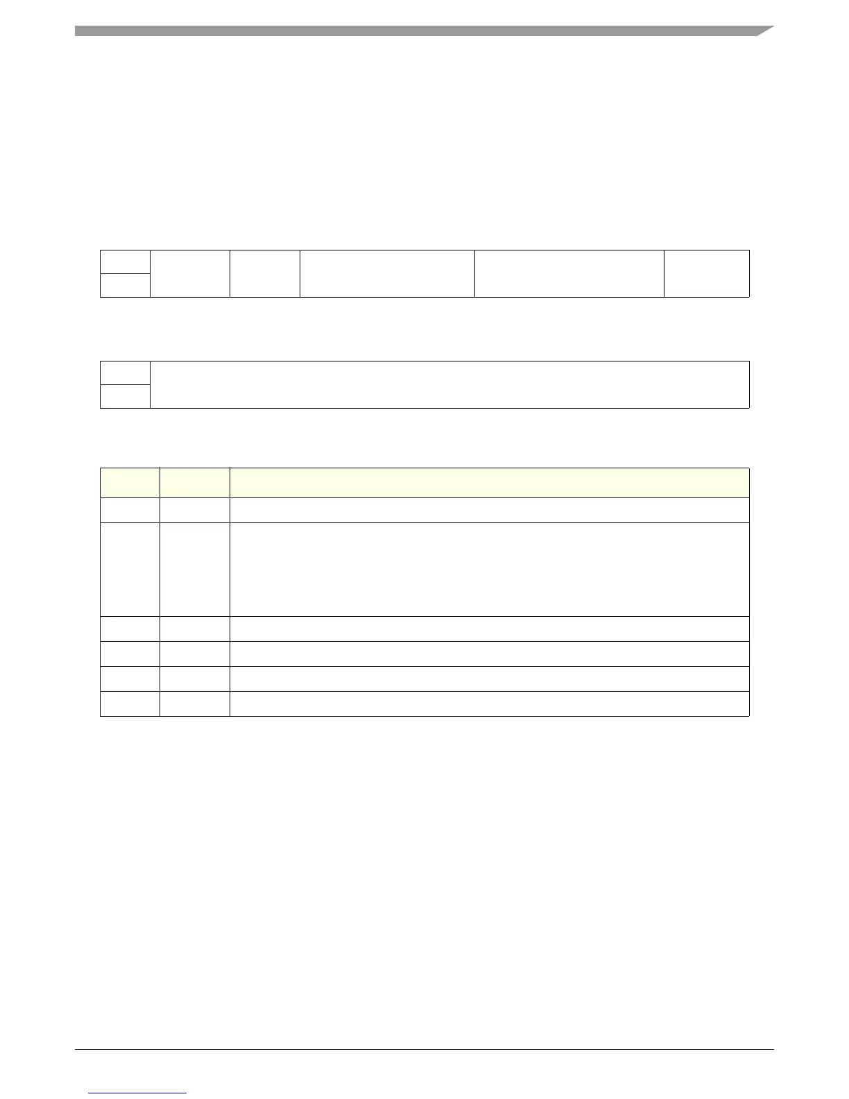
Table 14-15. FEC MII Management Frame Register
msb 012345678 9 1011121314 15
RST OP PA RA TA
W
RESET:X XXXXXXXX X X X XX X X
16 17 18 19 20 21 22 23 24 25 26 27 28 29 30 31 lsb
RDATA
W
RESET:X XXXXXXXX X X X XX X X
Bits Name Description
0:1 ST Start of Frame Delimiter—bits must be programmed to 01 for a valid MII management frame.
2:3 OP Operation Code—field must be programmed to 10 (read) or 01 (write) to generate a valid MII
management frame.
• A value of 11 causes a “read” frame operation.
• A value of 00 causes a “write” frame operation. However, these frames are not MII
compliant.
4:8 PA PHY Address—specifies 1 of up to 32 attached PHY devices.
9:13 RA Register Address—specifies 1 of up to 32 registers within the specified PHY device.
14:15 TA TurnAround—must be programmed to 10 to generate a valid MII management frame.
16:31 DATA Management Frame Data—used for data written to or read from PHY register.