MPC5200B Users Guide, Rev. 1
8-26 Freescale Semiconductor
Memory Controller Registers (MBAR+0x0100:0x010C)
MEM_CLK2—double frequency of MEM_CLK—DDR uses both edges of the bus-frequency clock (MEM_CLK) to read/write
data.
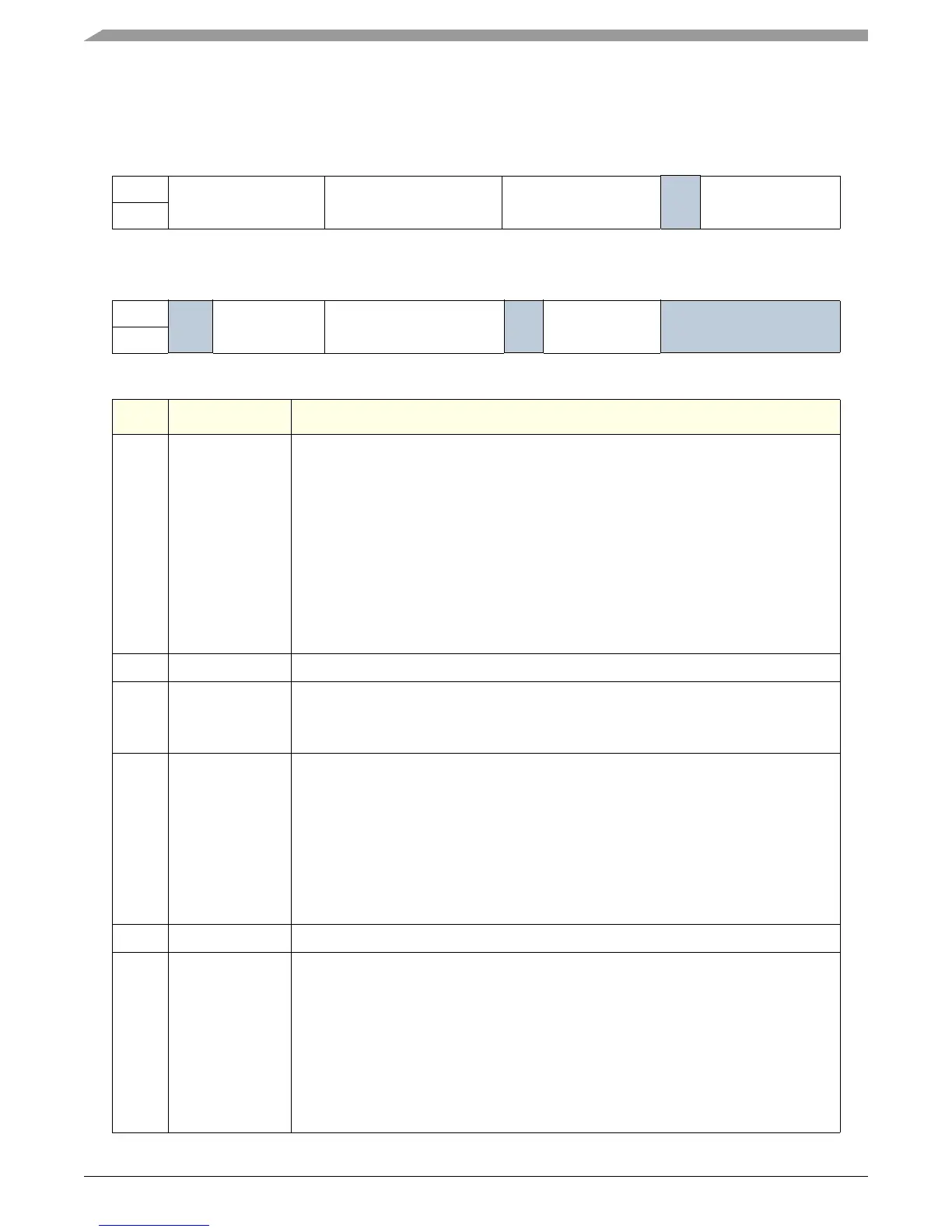
Table 8-10. Memory Controller Configuration Register 1
msb 01 2 3 4 5 6 7 8 9 101112 13 14 15
R srd2rwp swt2rwp rd_latency
Rsvd act2rw
W
RESET:00000 0 0 0 00000 0 0 0
16 17 18 19 20 21 22 23 24 25 26 27 28 29 30 31 lsb
R
Rsvd pre2act ref2act Rsvd wr_latency Reserved
W
RESET:0 0000 0 0 0 00000 0 0 0
Bit Name Description
0:3 srd2rwp Single Read to Read/Write/Precharge delay. Limiting case is Read to Write:
For DDR: CL + round trip delay + t
Hz
; round up.
If round trip delay = 1 clk and t
Hz
= 0.75 ns::
If CL==2: 2 + 1 + 0.75 ns = 3 clk + 0.75 ns, round to 0x3.
If CL==2.5: 2.5 + 1 + 0.75 ns = 3.5 clk + 0.75ns, round to 0x4
For SDR: CL + round trip delay + t
Hz
+ 1; round up.
If round trip delay = 1 clk and t
Hz
= 5.4 ns:
If CL==2: 2 + 1 + 5.4ns + 1 = 4 clk + 5.4ns, round to 0x5.
If CL==3: 3 + 1 + 5.4ns + 1 = 5 clk + 5.4ns, round to 0x6.
4—Reserved
4:7 swt2rwp Single Write to Read/Write/Precharge delay. Limiting case is Write to Precharge.
For DDR, suggested value = 0x3 (t
WR
+ 1 clk)
For SDR, suggested value = 0x2 (t
WR
)
8:11 rd_latency Read CAS Latency.
For DDR:
If CL==2, write 0x6
If CL==2.5, write 0x7
For SDR:
If CL==2, write 0x2
If CL==3, write 0x3
Note: NOTE: CL=2.5 is not supported for SDR.
12 — Reserved
13:15 act2rw Active to Read/Write delay.
Suggested value at 132 MHz = 0x02
Rule: t
RCD
/MEM_CLK-1. Round up to nearest integer.
EXAMPLE:
If t
RCD
= 20ns and MEM_CLK = 99 MHz
20ns / 10.1 ns = 1.98; round to 2; write 0x1.
If t
RCD
= 20 ns and MEM_CLK = 132 MHz
20ns / 7.5 ns = 2.66; round to 3; write 0x2.