MPC5200B Users Guide, Rev. 1
19-10 Freescale Semiconductor
Memory Map / Register Definition
19.5.7 MSCAN Receiver Flag Register (CANRFLG)—MBAR+0x0908 / 0x988
Note: This register is held in the reset state when the initialization mode is active (INITRQ = 1 and INITAK = 1). This register is
writable again as soon as the initialization mode is exited (INITRQ = 0 and INITAK = 0).
A flag can only be cleared when the condition which caused the setting is no longer valid and can only be cleared by software (writing a “1”
to the corresponding bit position). Every flag has an associated interrupt enable bit in the MSCAN Receive Interrupt Enable Register.
Read: Anytime
Write: Anytime when out of initialization mode, except RSTAT(1:0) & TSTAT(1:0) flags which are read only; write of “1” clears flag; write
of “0” ignored.
00114 Tq clock cycles
...................................................................................................................................
111015 Tq clock cycles
111116 Tq clock cycles
Table 19-9. Time Segment 2 Values
TSEG22 TSEG21 TSEG20 Time segment 2
0 0 0 1 Tq clock cycle (a)
0 0 1 2 Tq clock cycles
....................................................................................................................................
1 1 0 7 Tq clock cycles
1 1 1 8 Tq clock cycles
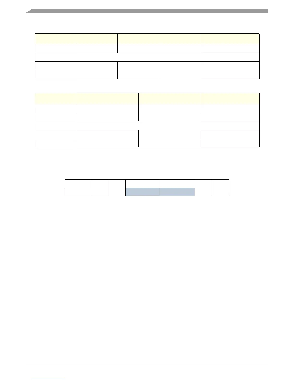
Table 19-10. MSCAN Receiver Flag Register
msb 01234567 lsb
R
WUPIF
CSCIF
RSTAT[1:0] TSTAT[1:0]
OVRIF
RXF
W
RESET:00000000
Table 19-8. Time Segment 1 Values (continued)
TSEG13 TSEG12 TSEG11 TSEG10 Time segment 1