Because RFL™ and Hubbell® have a policy of continuous product improvement, we reserve the right to change designs and specifications without notice.
19.3.2 CONTROLS AND INDICATORS
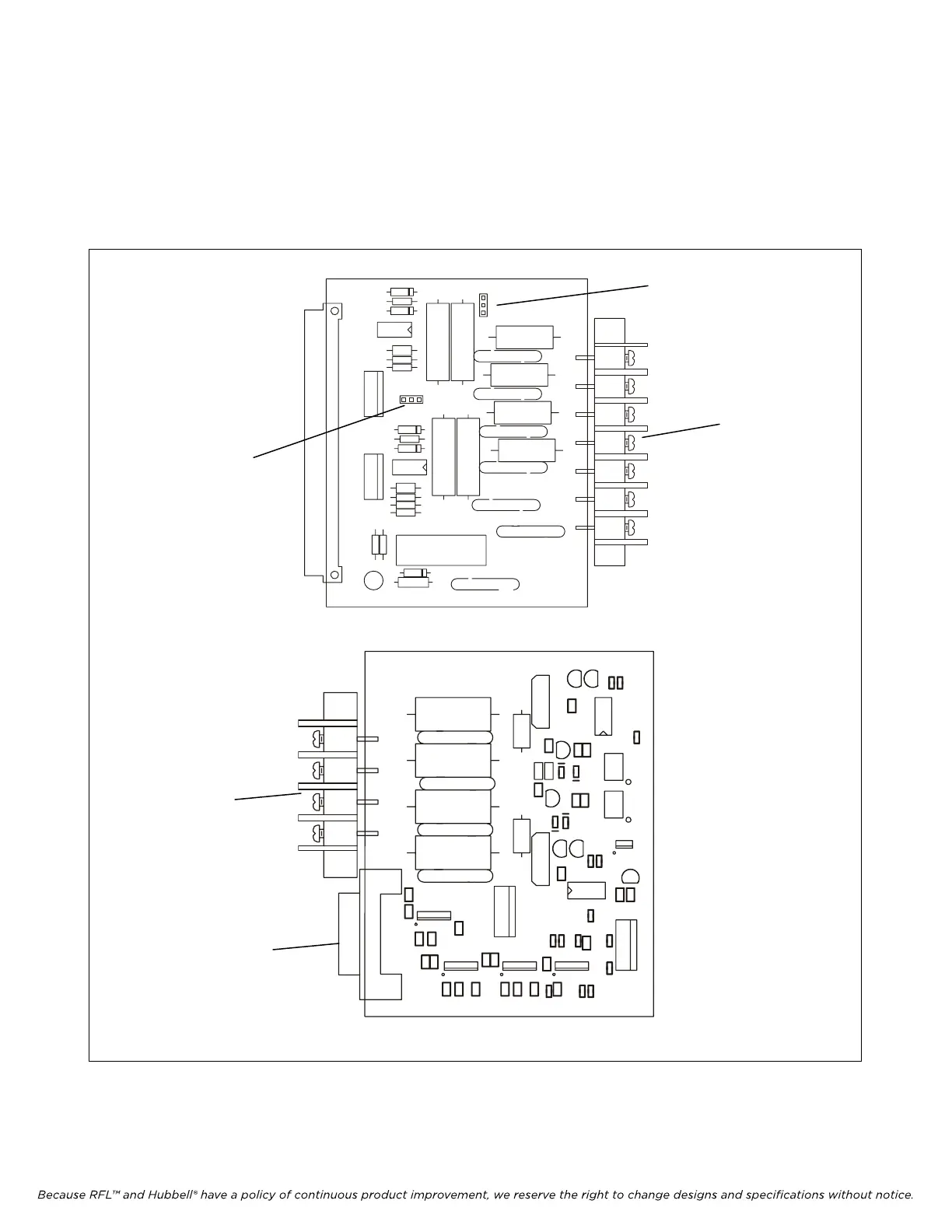
Figures 19-7 and 19-8 show the location of all controls and indicators on the Solid State Input/Output
I/O modules. These controls and indicators are described in Table 19-4. Only TB1, TB2 and P101 are
accessible with the Solid State Input/Output I/O module installed in the chassis. Jumpers J4 and J5 are
only accessible when the module is removed from the chassis or is on a card extender.
J9
J4
R20
TB1
L5
L6
L7
U2
R11
R15
R12
C8
C13
C15
C9
C10
C11
C12
CR9
CR10
CR11
CR12
R14
R13
R8
R7
R10
R19
C16
J8
R18
J5
L8
U1
R16
C7
C14
P1
K1
CR14
R9
R17
48V
125V
48V125V
1
+
SS INPUT I/O 106438-1 REV-B
1N4761A
1N4761A
N/A
N/A
N/A
11
3KV.01uF
J
1
0
9
C
1
0
1
Q
1
0
2
U110
C
1
3
9
C
1
3
2
C
1
3
1
U
1
0
9
P101
C
R
1
0
5
C
1
3
0
U106
C
1
1
5
Q104
C
1
1
9
U108
C
1
2
5
C
1
2
9
C
1
2
6
C
1
2
8
C
1
2
7
C
R
1
0
4
U107
C
1
2
0
C
1
2
4
Q
1
0
6
C
1
2
1
C
R
1
0
6
T
1
0
2
Q
1
0
1
R
1
0
6
J
1
0
8
C
1
1
1
C
1
1
4
C
1
1
3
T
B
2
U
1
0
5
L104
L102
L101
C
R
1
0
1
C
1
1
2
C
R
1
0
2
T
1
0
1
U104
Q103
Q
1
0
5
C
1
3
5
C
1
3
3
U
1
0
2
C103
C104
C105
C
1
3
4
R
1
1
1
R
1
1
2
C
1
1
6
C
R
1
0
3
U103
R
1
1
0
R
1
0
3
R
1
0
4
L103
C
1
0
2
R
1
0
2
C
1
2
3
C
1
1
8
U101
R
1
0
1
R
1
0
8
C106
R
1
0
9
R
1
0
5
C
1
1
7
C
1
2
2
J
P
1
0
2
R
1
0
7
J
P
1
0
1
C
1
3
6
C
1
3
7
9780/85 SS OUTPUT I/O 106643 REV-B
BOONTON, NJ, USA 2000
RFL ELECTRONICS INC.,
S
D
G
1
S
D
G
1
J4
J5
TB-1
TB-2
P101
Figure 19-7. Controls/indicators, Solid State Input/Output I/O Modules (Assy. No. 106635-1 and -2)
RFL 9785 RFL E
lectronics Inc.
September 1, 2006
19-12 (973) 334-3100