Because RFL™ and Hubbell® have a policy of continuous product improvement, we reserve the right to change designs and specifications without notice.
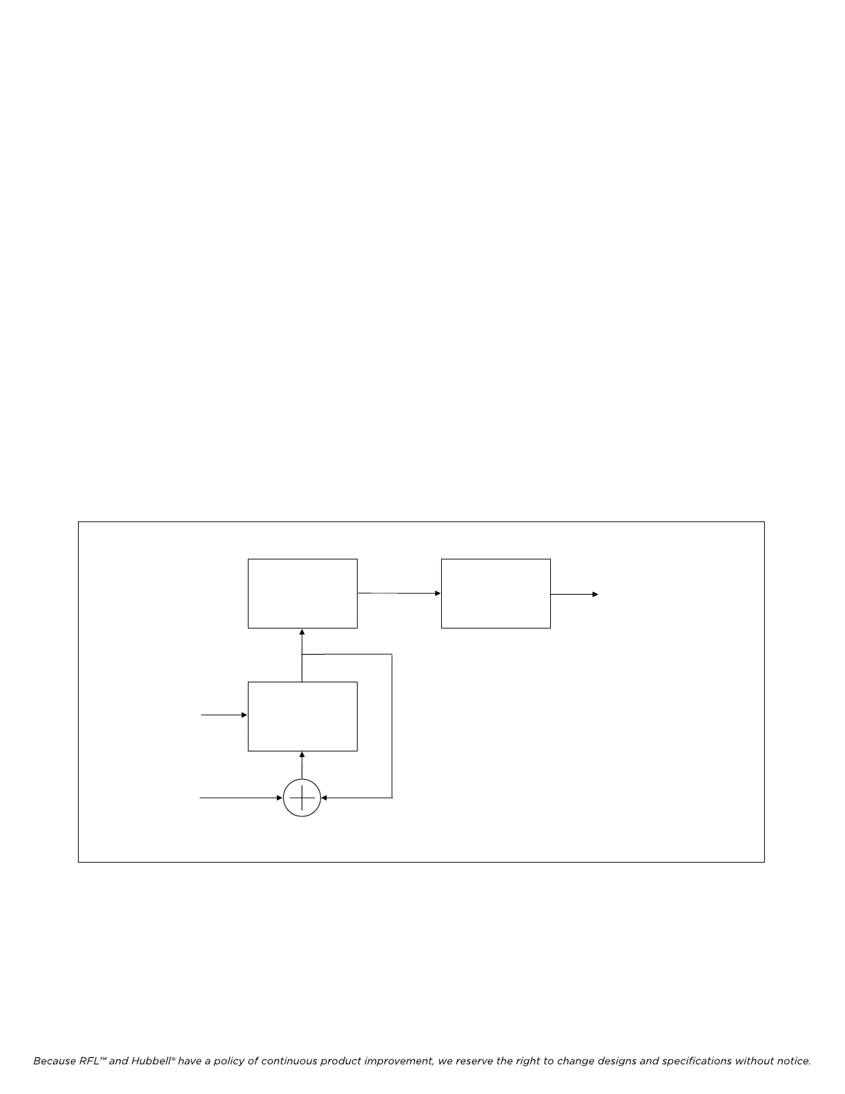
7.3.2 9785 DIRECT DIGITAL SYNTHESIZER
In the RFL 9785, the master clock frequency is a precision 50 MHz signal providing nearly 100 points
per cycle at the maximum output frequency. The phase accumulator is a 32 bit register which provides
over 4 billion possible phase values. This results in a very clean output from the DDS circuit.
All of the DDS functions are performed in a single integrated circuit, U1, which has a differential
current mode output. Resistors R3 and R4 are used for current to voltage conversion. U3C is
configured as a differential amplifier to convert the output of U1 to a single ended signal.
7.3.3 VOICE AMPLITUDE MODULATION
When the voice option is installed, U2A is used to modulate the reference input to the D/A portion of
the DDS based upon the voice input. This varies the full-scale setting of the D/A, thus providing the
desired modulation. The modulation can be disabled, by opening the analog switch U6D.
7.3.4 ANTI-ALIASING FILTER
The output of the DDS, after being converted to a single ended signal, is fed into an anti-aliasing filter
formed by U3D. The filter has a cutoff frequency of approximately 600 kHz.
U
P
D
A
T
E
Phase
Register
Sine Lookup
Table
D/A
Converter
Analog
Out
Master
Clock
Phase
Step
Figure 7-3. Block diagram of a basic DDS
RFL 9785 RFL E
lectronics Inc.
April 25, 2005 7-4 (973) 334-3100