Technical Specifications
7-23
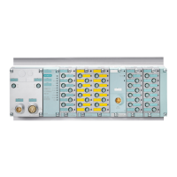
ET 200X Distributed I/O Device
EWA 4NEB 780601602-06
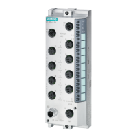
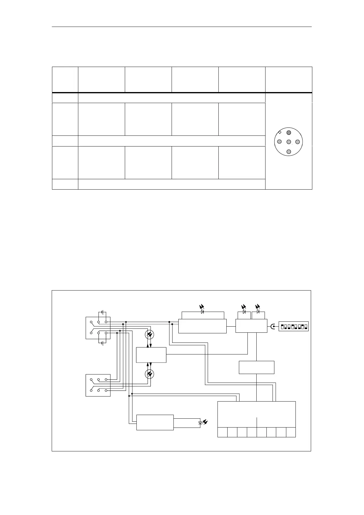
Table 7-11 Pinout of sockets X2, X4, X6 and X8 for digital inputs or outputs
Pin Assignment
of socket X2
Assignment
of socket X4
Assignment
of socket X6
Assignment
of socket X8
Front view of
socket
(Front view)
1 Non-switched supply voltage DC 24V-NS
2 Diagnostics
input or input
with NC
functionality
Diagnostics
input or input
with NC
functionality
Diagnostics
input or input
with NC
functionality
Diagnostics
input or input
with NC
functionality
2
3 Chassis ground, power supply
1
2
3
5
4* Digital input or
output
(DESINA)
channel 1
Digital input or
output
(DESINA)
channel 3
Digital input or
output
(DESINA)
channel 5
Digital input or
output
(DESINA)
channel 7
4
5 not assigned
* If it is parameterized as a digital output, pin 4 is fed by the DC 24V-NS non-switched supply voltage.
Covering up unused connections
You must seal off any connections which are not required with M12 screw caps, in
order to ensure that the degree of protection (IP 65, IP 66 or IP 67) is achieved.
Basic circuit diagram
The basic circuit diagram of the basic module is shown below.
DC 24 V-NS
PROFIBUS
address
Electronic
components
Internal power
supply
DC 24 V-NS RUN
A
Backplane bus
DC 24 V-S
Load voltage
monitor
SF
FO
interface
Parameterizable digital inputs
and outputs
X1 X3 X5 X7 X2 X4 X6 X8
B
DC 24 V-S
521
634
B
A
634
521
DESINA
connector
DC 24V-S
(for digital outputs)
DC 24 V-NS
X01
X02
Figure 7-5 Basic circuit diagram of the BM 143-DESINA FO basic module