System Control
ARM DDI 0388I Copyright © 2008-2012 ARM. All rights reserved. 4-32
ID073015 Non-Confidential
Table 4-38 shows the SDER bit assignments.
To access the SDER, read or write the CP15 register with:
MRC p15,0,<Rd>,c1,c1,1; Read Secure debug enable Register
MCR p15,0,<Rd>,c1,c1,1; Write Secure debug enable Register
4.3.13 Non-secure Access Control Register
The NSACR characteristics are:
Purpose Sets the Non-secure access permission for coprocessors.
Usage constraints The NSACR is:
• only accessible in privileged modes
• a read/write register in Secure state
• a read-only register in Non-secure state.
This register has no effect on Non-secure access permissions for the debug
control coprocessor, or the system control coprocessor.
Configurations Available in all configurations.
Attributes See the register summary in Table 4-3 on page 4-6.
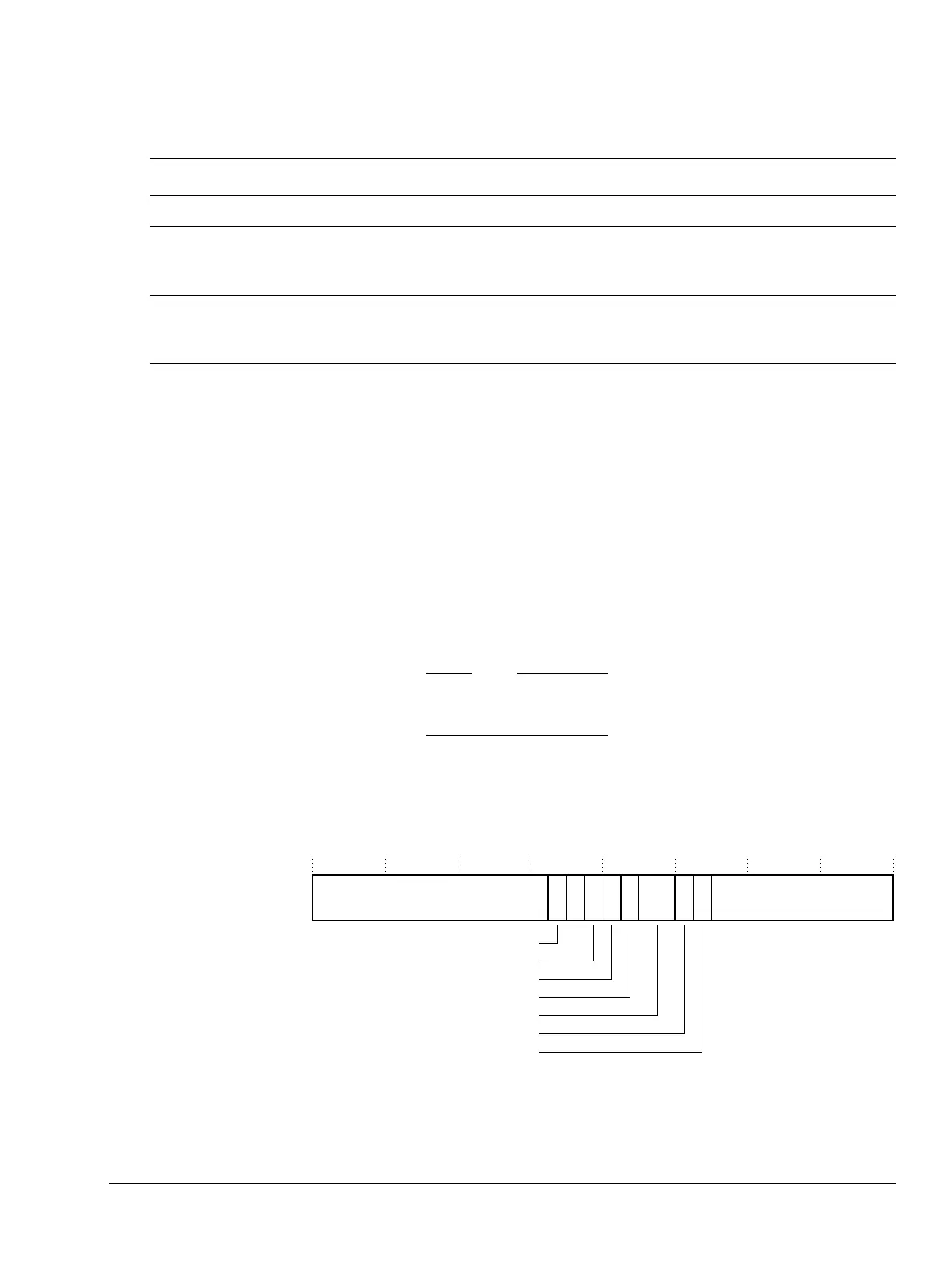
Figure 4-12 shows the NSACR bit assignments.
Figure 4-12 NSACR bit assignments
Table 4-38 SDER bit assignments
Bits Name Function
[31:2] - Reserved.
[1] Secure User Non-invasive Debug Enable 0 Non-invasive debug not permitted in Secure User mode.
This is the reset value.
1 Non-invasive debug permitted in Secure User mode.
[0] Secure User Invasive Debug Enable 0 Invasive debug not permitted in Secure User mode.
This is the reset value.
1 Invasive debug permitted in Secure User mode.
31 19 18 17 16 12 11 10 9 0
UNK/SBZP
CP11
CP10
T
L
UNK/SBZP
15
UNK/SBZP
14 13
NSASEDIS
NSD32DIS
NS_SMP
PLE