MPC5200B Users Guide, Rev. 1
2-68 Freescale Semiconductor
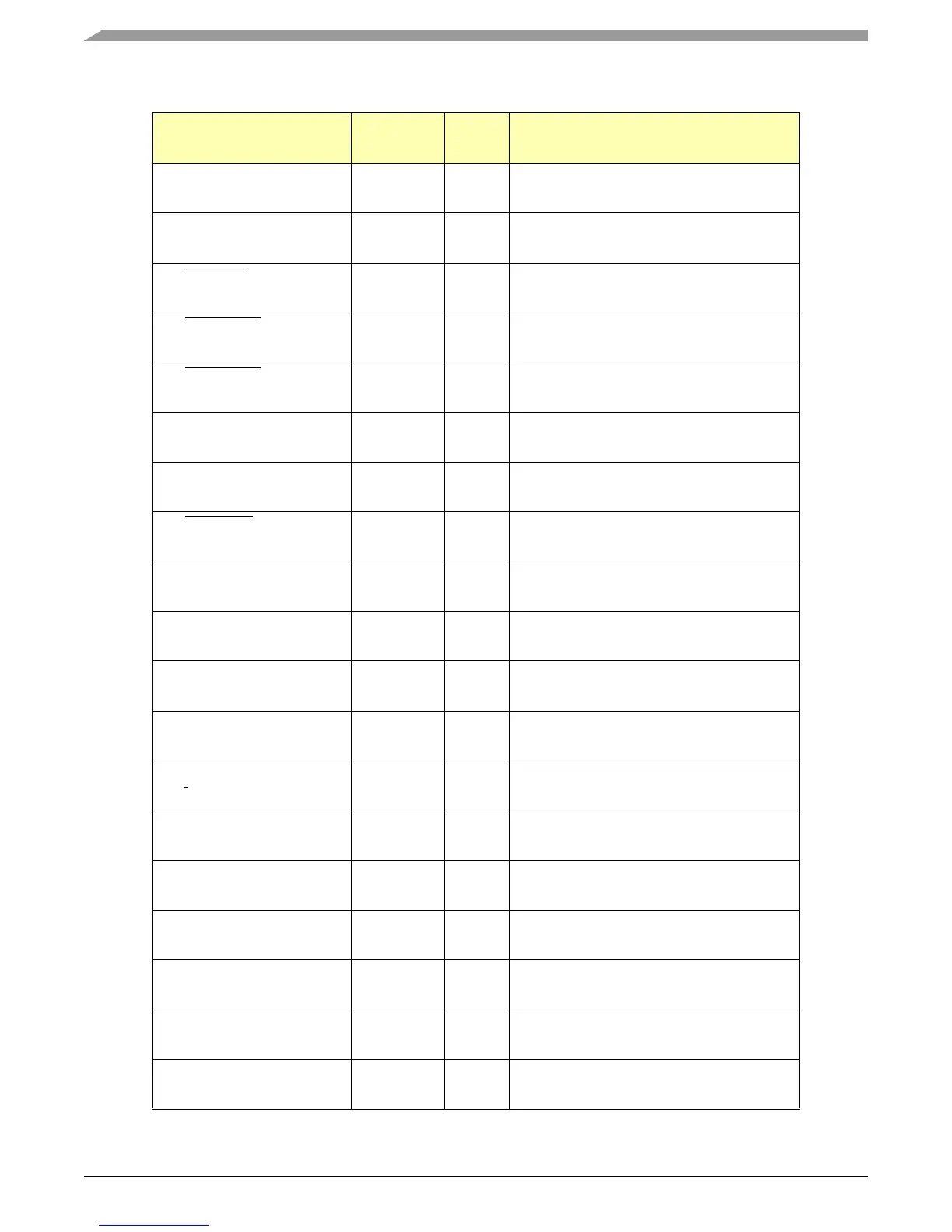
Pinout Tables
Table 2-27. SDRAM Bus Pin Functions
PIN BALL NUMBER Function
Reset
Value
Description
Pin MEM_RAS
Ball A18
logic 0 SDRAM Bus Row Address Strobe
Pin MEM_CAS
Ball B19
logic 0 SDRAM Bus Column Address Strobe
Pin MEM_WE
Ball A19
logic 0 SDRAM Bus Write enable
Pin MEM_CS_0
Ball B18
logic 1 SDRAM Bus Chip Select 0
Pin MEM_CS_1
Ball C15 (GPIO_WKUP_6)
logic 1 SDRAM Bus Chip Select 1
(shared with GPIO_WKUP_6)
Pin MEM_CLK_EN
Ball F20
logic 0 SDRAM Bus Clock Enable
Pin MEM_CLK
Ball G19
logic 0 SDRAM Bus Memory Clock
Pin MEM_CLK
Ball G20
logic 1 SDRAM Bus Inverted Memory Clock
Pin MEM_MBA_1
Ball A17
logic 0 SDRAM Bus Memory Bank Address 1
Pin MEM_MBA_0
Ball C18
logic 0 SDRAM Bus Memory Bank Address 0
Pin MEM_MDQS_3
Ball L18
hi - z SDRAM Bus Bidirectional Data Bus Strobe 3
Pin MEM_MDQS_2
Ball D18
hi - z SDRAM Bus Bidirectional Data Bus Strobe 2
Pin MEM_MDQS_1
Ball
H20
hi - z SDRAM Bus Bidirectional Data Bus Strobe 1
Pin MEM_MDQS_0
Ball N20
hi - z SDRAM Bus Bidirectional Data Bus Strobe 0
Pin MEM_DQM_3
Ball L17
SDRAM Bus Data Mask 3
Pin MEM_DQM_2
Ball A20
SDRAM Bus Data Mask 2
Pin MEM_DQM_1
Ball H19
SDRAM Bus Data Mask 1
Pin MEM_DQM_0
Ball N19
SDRAM Bus Data Mask 0
Pin MEM_MA_12
Ball F19
logic 0 SDRAM Bus Memory Address 12