Memory Controller Registers (MBAR+0x0100:0x010C)
MPC5200B Users Guide, Rev. 1
Freescale Semiconductor 8-29
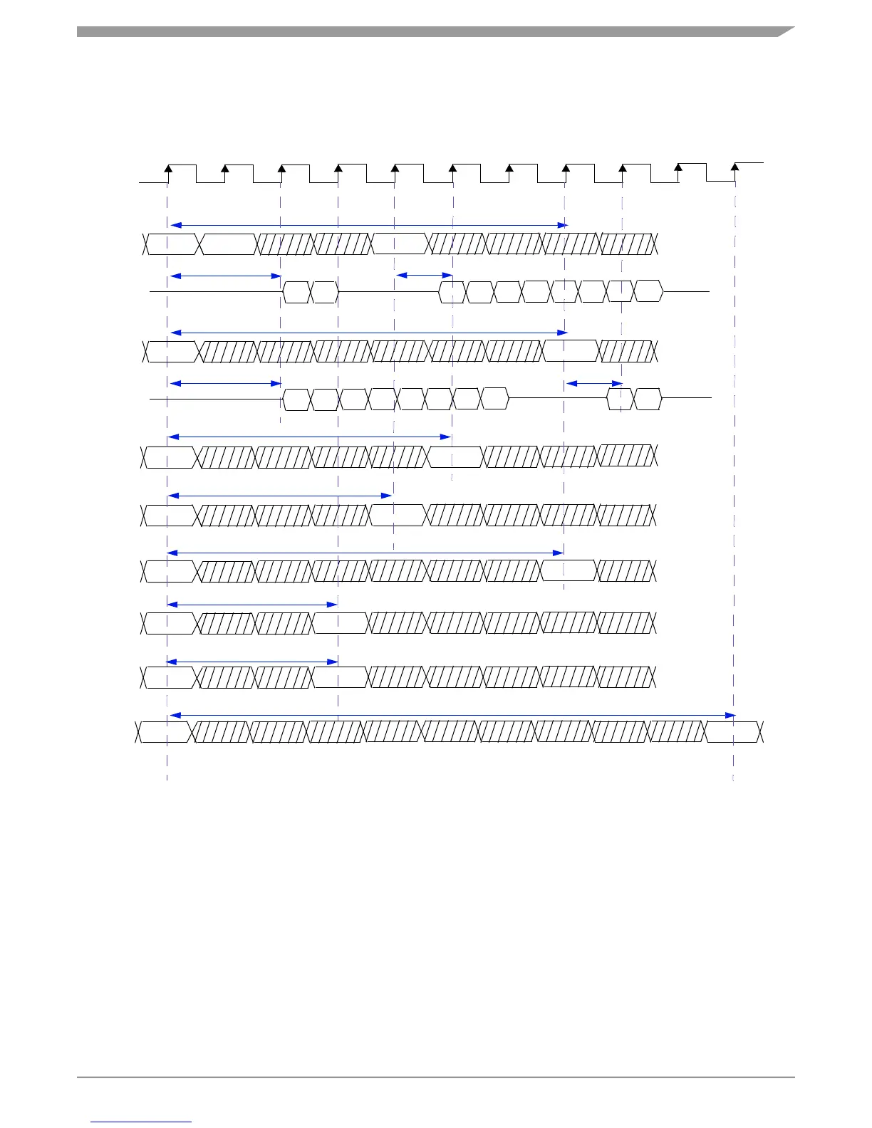
The Figure 8-3. Programmable Command Timings shows the timings which can be programmed by the two Controller Configuration
Register. The timing diagram uses the suggested values for a DDR memory and a 132 MHz memory clock. The displayed Commands are the
limiting cases.
Figure 8-3. Programmable Command Timings
MEM_CLK
Burst Read to Read
Read
Read
Single Read to Read/Write/Precharge
Read
Bstrm
Write
Prech
Write
Prech
Single Write to Read/Write/Precharge
Burst Write to Read/Write/Precharge
Data
Prech
Precharge to Active/Refresh
Active
Ref
Refresh to Active
Active
(srd2rwp +1)
CL
brd2rp + 1
swt2rwp + 1
bwt2rwp + 1
pre2act + 1
ref2act + 1
Active
Active to Read/Write
Read
act2rw + 1
wr_latency/3
Read
Write
Data
(srd2rwp +1) or (brd2wt + 1)
CL
Burst Read to Write/Precharge
wr_latency/3
Write