MPC5200B Users Guide, Rev. 1
18-16 Freescale Semiconductor
I
2
C Interface Registers
18.3.5 I
2
C Data I/O Register (MDR)—MBAR+ x3D10 / 0x3D50
5 SRW Slave Read/Write—when set, bit indicates the R/W command bit value of the calling address sent
from the master.
BE AWARE: Bit is valid only when I
2
C is in slave mode, a complete address transfer occurred with
an address match, and no other transfers were initiated. Checking this bit, the CPU can select
slave Tx/Rx mode according to the master command.
0 = Slave receive, master writing to slave
1 = Slave transmit, master reading from slave
6IFI
2
C Interrupt—sets when an interrupt is pending. If IEN is set, a processor interrupt request is
generated. IF sets when one of the following events occurs:
1. Complete 1Byte transfer (set at falling edge of 9th clock).
2. A Rx calling address matches its own specific address in slave mode.
3. Arbitration is lost.
This bit must be cleared by software writing it low in the interrupt routine.
7 RXAK Receive Acknowledge—SDA value during the bus cycle acknowledge bit.
• If bit is low, it indicates an acknowledge signal was received after completion of 8 bits of data
transmission on the bus.
• If bit is high, it means no acknowledge signal is detected at the 9th clock.
0 = Acknowledge received
1 = No acknowledge received
8:31 — Reserved
Note: This status register is read-only with the exception of bit6 (IF), bit4 (AKF) and bit3 (AL), which are software
clearable.
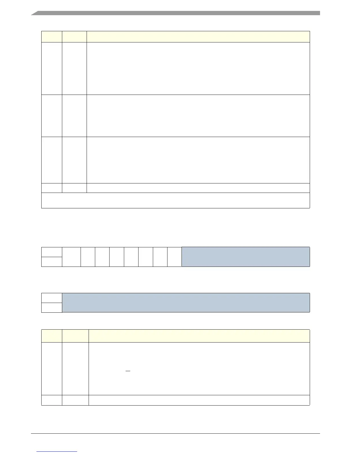
Table 18-7. I
2
C Data I/O Register
msb 012345678 9 1011121314 15
R D7 D6D5D4D3D2D1D0
Reserved
W
RESET:0 00000000 0 0 0 00 0 0
16 17 18 19 20 21 22 23 24 25 26 27 28 29 30 31 lsb
R
Reserved
W
RESET:0 00000000 0 0 0 00 0 0
Bit Name Description
0:7 D[7:0] In Master Transmit Mode—when data is written to this register, a data transfer is initiated. The
most significant bit is sent first.
Note: In this mode, the first data byte written to DR. Assertion of STA is used for the address
transfer and should be comprise of the calling address (in position D[7]:D[1]) concatenated with
the required R/W
bit (in position D0).
In Master Receive Mode—reading this register initiates next byte data receiving.
In Slave Mode—the same functions are available after an address match occurs.
8:31 — Reserved
Bit Name Description