10 - 5
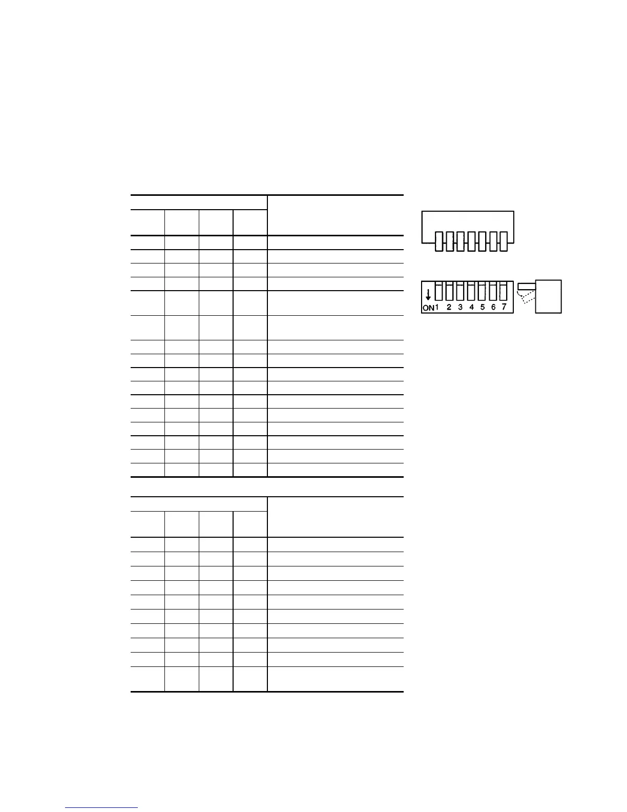
(3) Setting of DIP Switch
The DIP switch on the front panel is divided into operation mode setting part (SW1, 2, 3,
4) which determines operation at startup of the CPU board and program boot I/O setting
part (SW5, 6, 7, 8). This switch setting is reflected on the system status register on the
CPU board and can be read via software.
Explanation of SW1 Bits External View of DIP Switch
Switch No./Bit
SW1
D7
SW2
D6
SW3
D5
SW4
D4
Operation Mode
0 0 0 0 Normal processing mode
0 0 0 1 Reserve
0 0 1 0 Reserve
0 0 1 1 Reserve
0 1 0 0 Continuous processing mode
(memory BRAM)
0 1 0 1 Continuous processing mode
(EEPROM)
0 1 1 0 Reserve
0 1 1 1 Reserve
1 0 0 0 Reserve
1 0 0 1 Reserve
1 0 1 0 Reserve
1 0 1 1 Reserve
1 1 0 0 T/M mode 1
1 1 0 1 T/M mode 2
1 1 1 0 T/M mode 3
1 1 1 1 T/M mode 4
Switch No./Bit
SW5
D3
SW6
D2
SW7
D1
SW8
D0
Boot I/O
0 0 0 SCSI device (H/D, etc.)
0 0 1 F/D
0 1 0 Reserve
0 1 1 Reserve
1 0 0 Reserve
1 0 1 I/O file ROM
1 1 0 EEPROM
1 1 1 Ethernet
0
Memory dump with boot I/O
1
Memory dump with any other
than boot I/O