14 - 3
14.1.3 ADC Timing Adjustment
Adjust the ADC timing in the following procedure.
< Adjusting procedure >
The board to be adjusted is the DI board (1st board from the right in circuit board rack).
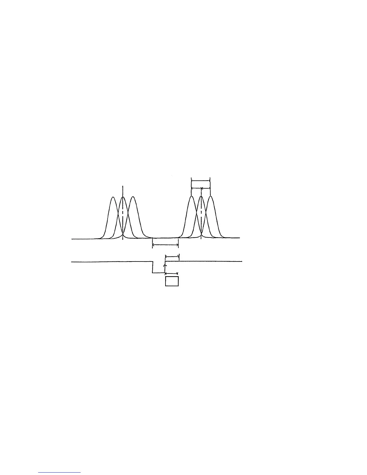
(1) Measure voltage across check pins TP1-TP2 (G) (DI board) and across TP14-GND (LOG
AMP board) using a synchroscope.
(2) Rotate the reaction disk using the mechanism check operation of the instrument check
program, and adjust the measured waveform using trimmer VR1 to obtain the timing
shown in Fig. 14-1.
NOTE: It may take 1 or 2 minutes until the LOG AMP output waveform appears.
Fig. 14-1 ADC Timing Waveform Specification
14.1.4 Reaction Bath Temperature Adjustment
Adjust reaction bath temperature in the following procedure.
< Adjusting procedure >
(1) Connect a tester across CP5 and SG of EMIO100 board.
(2) Turn power on and put the instrument in standby.
15 ms or more (flat section)
One shot in DI
LOG output
* Terminals:
Between TP14 and AG
In AD converting operation, a time period of 13 ms is
taken from the rise of ADC start signal. This period of
time should correspond to the flat section of LOG
output.
LOG output:
Across LOG AMP board TP14-GND
Across DI board TP1-TP2
(adjust with VR1)
26 ms
13 ms
±4 ms
-4 +4
A/D
* Terminals:
Between TP1 and DG