7: BASIC INSTRUCTIONS
USER’S MANUAL 7-23
SFR and SFRN (Forward and Reverse Shift Register)
The shift register consists of a total of 64 bits which are allocated to R0 through R63 in the standard processing mode. In
the high-speed processing mode, 32 bits are available for the shift register allocated to R0 through R31. Any number of
available bits can be selected to form a train of bits which store on or off status. The on/off data of constituent bits is
shifted in the forward direction (forward shift register) or in the reverse direction (reverse shift register) when a pulse input
is turned on.
Forward Shift Register (SFR)
When SFR instructions are programmed, two addresses are always required. The SFR instruction is keyed, followed by a
shift register number selected from appropriate operand numbers. The shift register number corresponds to the first, or
head bit. The number of bits is the second required address after the SFR instruction.
The SFR instruction requires three inputs. The forward shift register circuit must be programmed in the following order:
reset input, pulse input, data input, and the SFR instruction, followed by two required addresses.
Reset Input
The reset input will cause the value of each bit of the shift register to return to zero. Initialize pulse special internal relay,
M301, may be used to initialize the shift register at start-up.
Pulse Input
The pulse input triggers the data to shift. The shift is in the forward direction for a forward shift register and in reverse for
a reverse shift register. A data shift will occur upon the leading edge of a pulse; that is, when the pulse turns on. If the pulse
has been on and stays on, no data shift will occur.
Data Input
The data input is the information which is shifted into the first bit when a forward data shift occurs, or into the last bit
when a reverse data shift occurs.
Note: When power is turned off, the statuses of all shift register bits are normally cleared. It is also possible to maintain the
statuses of shift register bits by setting FUN4 as required. See page 5-5.
Setting and Resetting Shift Register Bits
I1
I0
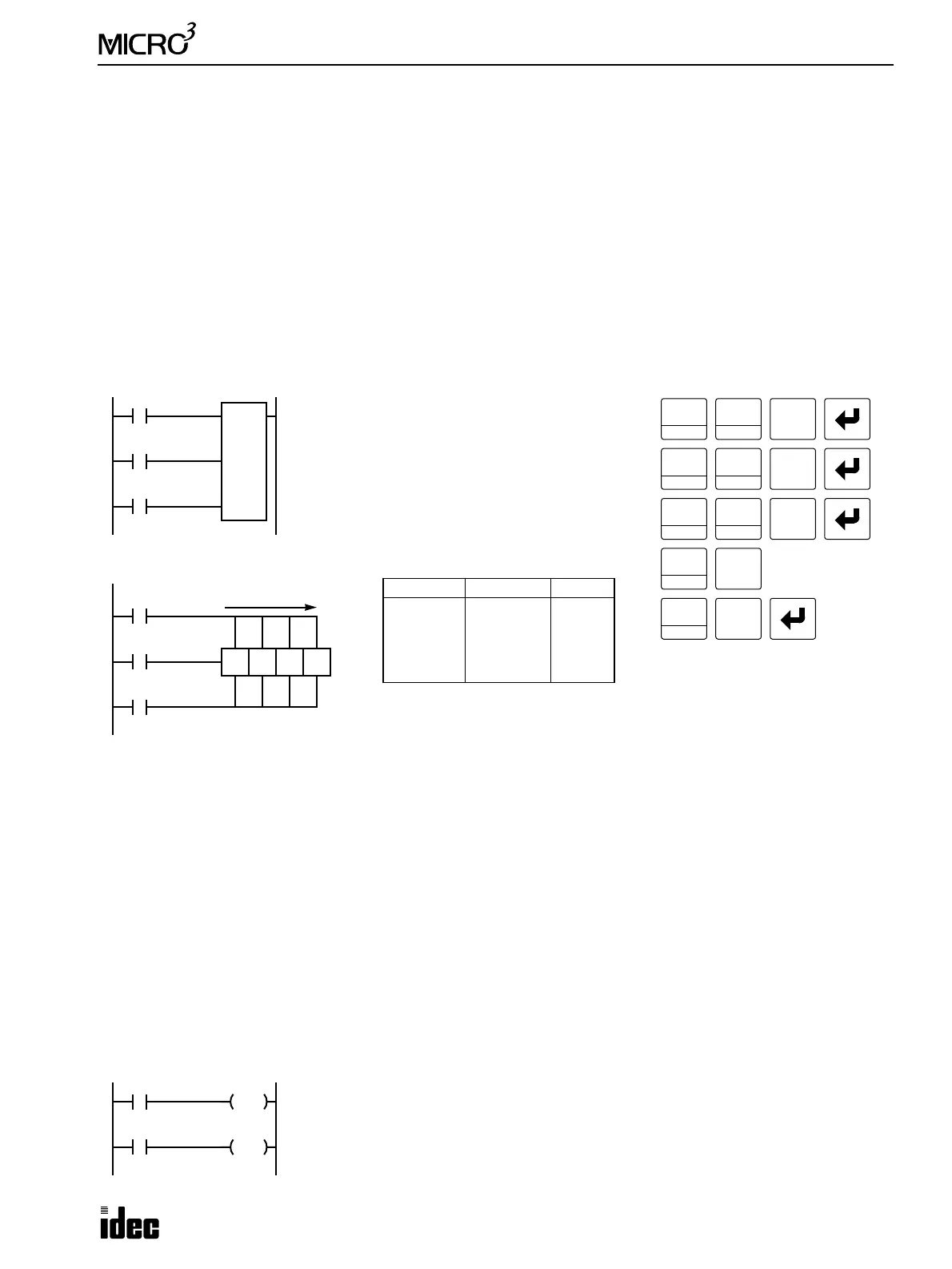
Ladder Diagram
Key Operation
LOD
10
SET
I
Prgm Adrs Instruction Data
0
1
2
3
LOD
LOD
LOD
SFR
I0
I1
I2
0
4
Program List
R0
4
1
BPS
0
Reset
Pulse
LOD
10
SET
I
LOD
10
2
BRD
0
I2
Data
LOD
10
SET
I
SFR
R
4
Structural Diagram
I2
I0
R0
Reset
Data
I1
Pulse
R1 R2 R3
Shift Direction
First Bit: 0 # of Bits: 4
First Bit: 0 to 63 (standard processing mode)
0 to 31 (high-speed processing mode)
# of Bits: 1 to 64 (standard processing mode)
1 to 32 (high-speed processing mode)
Note: To enter a decimal con-
stant as the number of bits,
press the LOD/10 key followed
by the number of bits.
I1
I0
R0
SET
R3
RST
• Any shift register bit can be turned on using the SET instruction.
• Any shift register bit can be turned off using the RST instruction.
• The SET or RST instruction is actuated by any input condition.