USER’S MANUAL 15-1
15: INTERFACE INSTRUCTIONS
Introduction
The DISP (display) instruction is used to display 1 through 5 digits of timer/counter current values and data register data
on 7-segment display units.
The DGRD (digital switch read) instruction is used to read 1 through 5 digits of digital switch settings to a data register or
16 internal relay points. This instruction is useful to change preset values for timers and counters using digital switches.
The ANR0 and ANR1 (analog read) instructions are used to read the analog value (0 through 255) set on the analog poten-
tiometer on the MICRO
3
base unit to a data register.
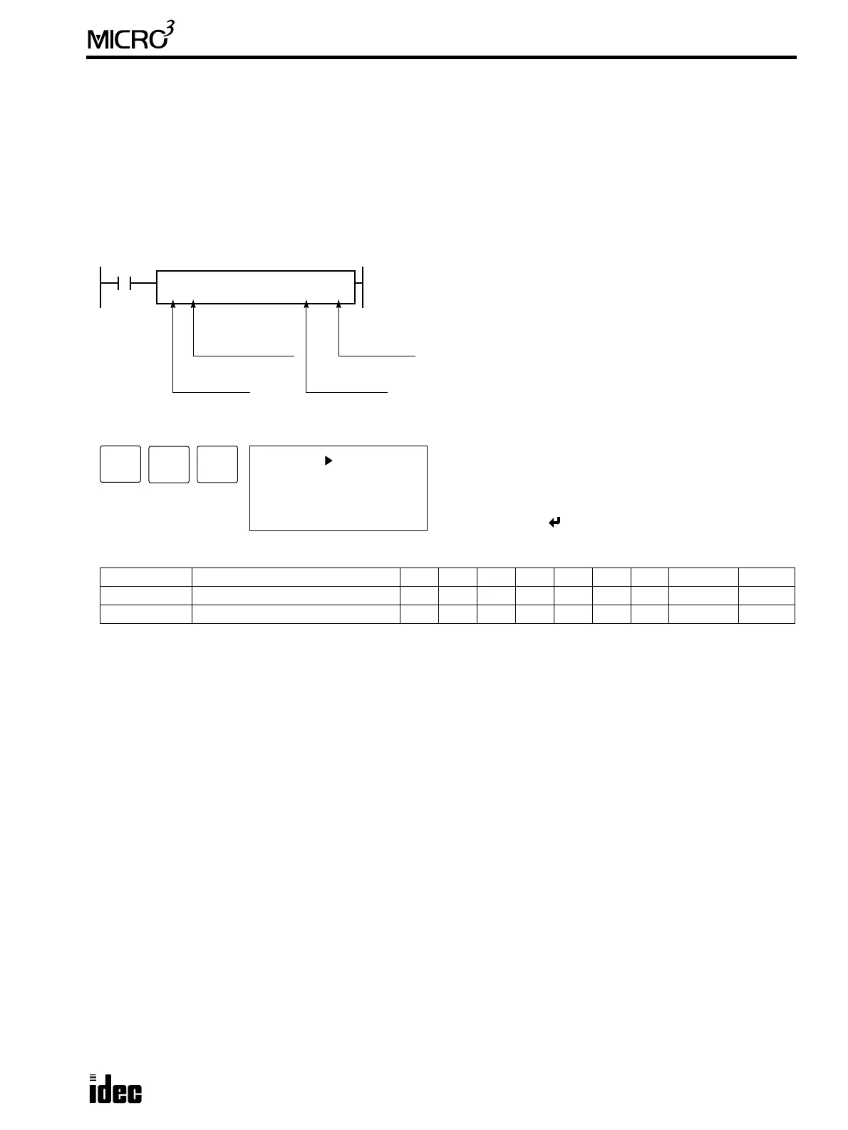
81 DISP (Display)
Key Operation
Valid Operands (Standard Processing)
In the high-speed processing mode, operands for advanced instructions are limited. See page 6-1.
When T (timer) or C (counter) is used as S1, the timer/counter current value is read out.
Conversion
BCD: To connect decimal display units
BIN: To connect hexadecimal display units
Latch Phase and Data Phase
Select the latch and data phases to match the phases of the display units in consideration of sink or source output of the
MICRO
3
base unit.
Output Points
The quantity of required output points is 4 plus the quantity of digits to display. When displaying the maximum of 5 digits,
9 consecutive output points must be reserved starting with the first output number designated by operand Q. Make sure
that actual output terminals are available for all output numbers. Do not let the output numbers straddle the base and
expansion stations in the expansion link system.
Display Processing Time
Displaying numerical data requires the following time after the input to the DISP instruction is turned on. Keep the input
to the DISP instruction for the period of time shown below to process the display data.
Operand Function I Q M T C R D Constant Repeat
S1 (Source 1) Data to display — — — 0-31 0-31 — 0-99 — —
Q First output number to display data — 0-25 ————— — —
Scan Time Display Processing Time
Less than 5 msec
5 msec or more
(10 msec + 1 scan time) × Quantity of digits
3 scan times × Quantity of digits
Latch phase:
Low or High
Data phase:
Low or High
Conversion:
BCD or BIN
Quantity of digits:
1 to 5
When input is on, data designated by source operand S1 is set
to outputs designated by operand Q. This instruction is used to
output 7-segment data to display units.
Note: The DISP instruction can be used on transistor output
type MICRO
3
base units only.
The DISP instruction can be used only once in a user program.
Display data can be 0 through 65535 (FFFFh).
DISP DATS1
****
Q
****
BCD4
LAT
LL
ADV
1
BPS
1 S1
DISP *BCD L:4
(Q: 0)
LATCH*L DATA*L
Enter operands S1, Q, and quantity of digits (1 to 5).
To select the conversion, latch phase, and data phase, press
the REP key.
To exit, press the key.
8
MCS/R