Board Design Guidelines for SmartFusion2 SoC and IGLOO2 FPGAs
AC393 Application Note Revision 14.0 14
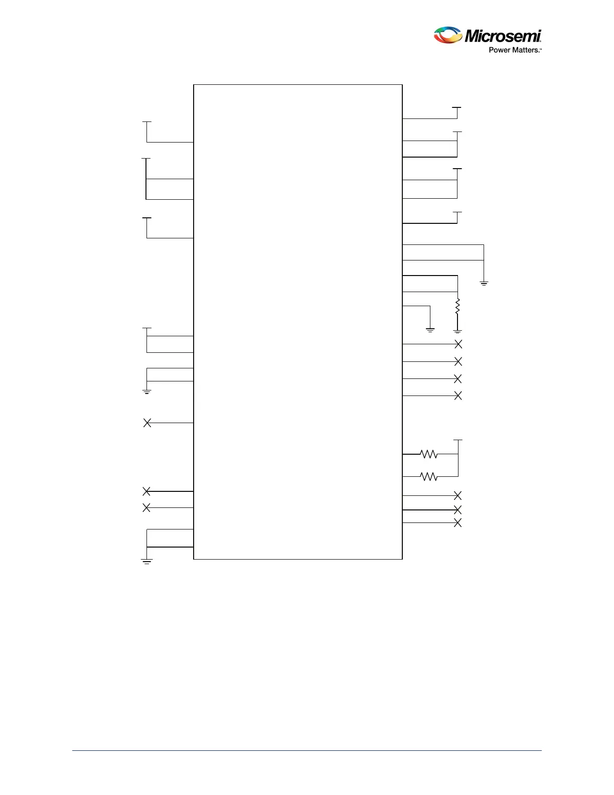
Figure 4 • Recommendations for Unused Pin Configurations
Note: For M2S090T(S), M2GL090T(S), M2S150T(S), and M2GL150T(S) devices, the VPP and VPPNVM must
be connected to a +3.3 V supply.
Note: SERDES_RXD pin connections are changed to VSS through a 10 kΩ resistor to reduce the latch-up risk.
This change does not effect the old board design functionality.
For recommendations on unused VDDI supplies, see the following tables.
SmartFusion2/IGLOO2 devices have multiple bank supplies. In cases where specific banks are not used,
Microsemi recommends connecting them as listed in the following tables.
If there is no recommendation provided for a device-bank supply combination, it means the bank is not
pinned out.
L23SERDES_x_ _VDDAIO
SERDES _x_L01_VDDAIO
SERDES _x_VDD
SERDES _x_L01_VDDAPLL
SERDES_x_L01_REFRET
SERDES _x_L 23_REXT
SERDES _x_L 23_VDDAPLL
SERDES_x_L23_REFRET
SERDES _x_L 01_REXT
SERDES _x_PLL _VDDA
SERDES _x_PLL _VSSA
CCC_xyz_PLL _VDDA
__ _CCC xyz PLL VSSA
MSS/HPMS_xDDR_PLL_VDDA
VPP
VPPNVM
VDD
1.2 V
S E R D E S _ x _T X D [3 :0] _P
SERDES _x_RXD[3:0]_P
S E R D E S _ x _R X D [3 :0]_ N
SERDES _x_TXD[3:0]_N
XTLOSC_[MAIN/AUX]_EXTAL
XTLOSC_[MAIN/AUX]_XTAL
SmartFusion2/IGLOO2
VSSNVM
VSS
MSIO
MSIOD
DDRIO
VREFx
DNC or VSS
JTAGSEL
JTAGTCK
Libero Defined DNC
1.2 V
1.2 V/2.5 V
VDDI(JTAG)
VDDIx
1.2 / 1.5 / 1.8 / 2.5 / 3.3 V
DNC
DNC
MSS/HPMS_xDDR_PLL_VSSA
VDD
2.5 V/3.3 V
1 kΩ
1 kΩ
2.5 V/3.3 V
2.5 V/3.3 V
10 kΩ