Board Design Guidelines for SmartFusion2 SoC and IGLOO2 FPGAs
AC393 Application Note Revision 14.0 31
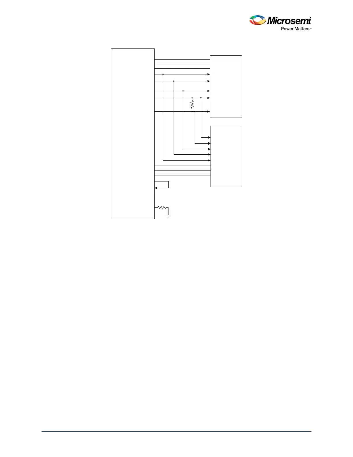
Figure 17 • LPDDR Interface
Note: Impedance calibration is optional for LPDDR operating in LVCMOS mode and is required for LPDDR1
operating in SSTL18 mode.
Note: For a 4- or 8-bit DRAM, all DQ pins are interchangeable. All 4- and 8-bit DQ pins are interchangeable in
LPDDR, DDR2, and DDR3 memories. For a 16-bit DRAM, DQ0 through DQ7 are interchangeable. Also,
DQ8 through DQ15 are interchangeable. However, DQ0-7 pins or signals must not be interchanged with
the DQ8-15 pins or signals.
Note: Short ECC_TMATCH_ OUT and ECC_TMATCH_ IN when using ECC bits.
SmartFusion2/IGLOO2
16 LPDDR SDRAM
x
16 LPDDR SDRAM
x
xDDR_CLK
xDDR_CLK_N
Control lines
CKE, CS, WE, RAS, CAS
xDDR_DQS [1:0]
xDDR_DM_RDQS [1:0]
xDDR_DQ [15:0]
xDDR_BA [2:0]
xDDR_ADDR [14:0]
xDDR_TMATCH_IN
xDDR_TMATCH_ECC_OUT
xDDR_TMATCH_ECC_IN
100
Ω
xDDR_IMP_CALIB_ECC
240Ω_1%
xDDR_DQS [3:2]
xDDR_DM_RDQS [3:2]
xDDR_DQ [31:16]
xDDR_TMATCH_OUT
 Loading...