Layout Guidelines for SmartFusion2- and IGLOO2-Based Board Design
AC393 Application Note Revision 14.0 50
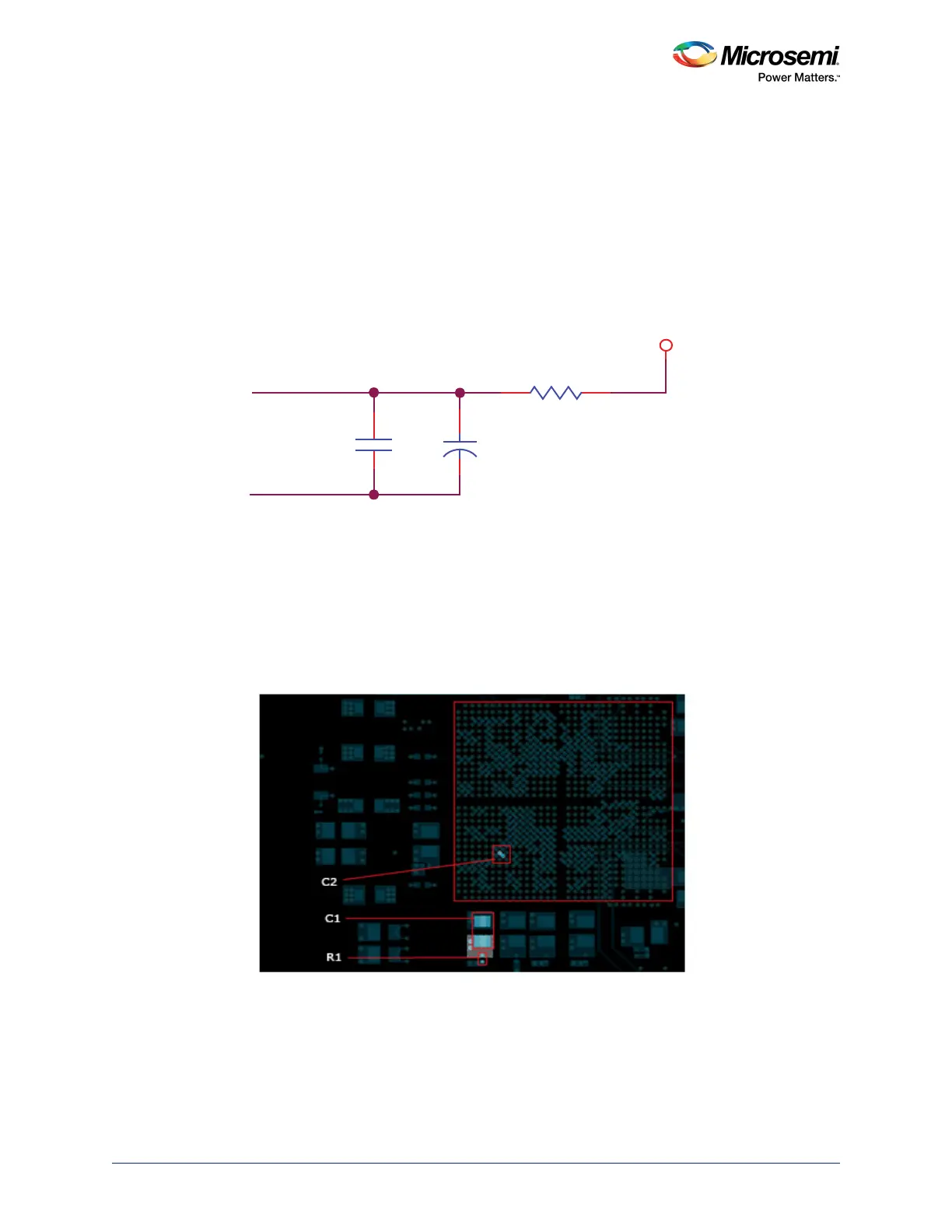
3.5 PLL
To achieve a reasonable level of long term jitter, it is vital to deliver an analog grade power supply to the
PLL. An R-C or R-L-C filter is used with the C being composed of multiple devices to achieve a wide
spectrum of noise absorption. Even the circuit is simple, there are specific board layout requirements.
Board layout around the high-frequency capacitor and the path to the pads are critical. It is vital that the
quiet ground and power are treated like analog signals. The entire VDDPLL and PLLVSSA wiring path
must not be coupled with any signal aggressors – especially, any high-swing and high-slew rate signals
such as TTL, CMOS, or SSTL signals used in DDR buses, and so on.
The recommended circuit for the power supply filter is shown in the following figure.
Figure 40 • Filter Circuit for PLL
For more information about R1, C1, and C2, see Board Design Guidelines for SmartFusion2 SoC and
IGLOO2 FPGAs, page 4.
3.5.1 Component Placement
• The capacitor (C1) and series resistor (R1) should be placed near the device as close as possible to
C2 device. A sample placement is shown in the following figure.
• The decoupling capacitor (C2) should be placed near the BGA via. The capacitor pad to via trace
should be as small as possible. For more information about R1, C1, and C2, see Board Design
Guidelines for SmartFusion2 SoC and IGLOO2 FPGAs, page 4.
Figure 41 • Placement of Capacitors for PLL filter Circuit
PLL_VDDA
PLL_VSSA
PLL_VDDA
R1
C1
C2
+
 Loading...