Board Design Guidelines for SmartFusion2 SoC and IGLOO2 FPGAs
AC393 Application Note Revision 14.0 30
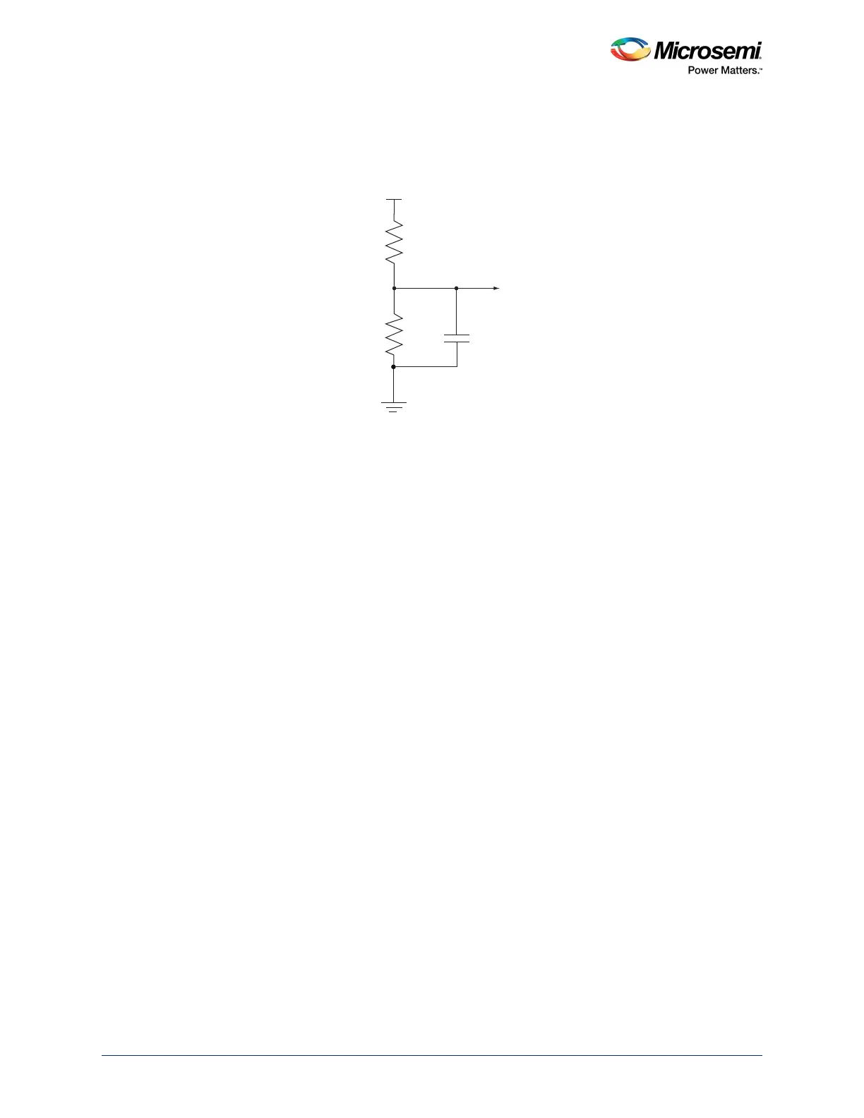
2.9.2 VREF Power
VREF is a low-power reference voltage equal to half of VDDQ. It must also be equal to VTT ± 40 mV. The
following figure shows the VREF generation circuit.
Figure 16 • VREF Generation
The following are the guidelines for connecting VREF power:
• For light loads (less than four DDR components), connect VDDQ to VSSQ through a simple resistor
divider composed of two equivalent 1% 1 kΩ resistors (Figure 16, page 30).
• Generate a local VREF at every device, rather than generating a single VREF with one divider and
routing it from the controller to the memory devices.
• Decouple at each device or connector to minimize noise.
Note: Use discrete resistors, not a resistor pack, to generate VREF.
2.9.3 VTT Power
VTT is memory bus termination voltage. To maintain noise margins, VTT must be equal to VDDQ/2, with
an accuracy of ± 3%. VTT terminates command and address signals to VDDQ/2 using a parallel resistor
(RT) tied to a low impedance source.
VTT is not used to terminate any DDR clock pairs. Rather, the xDDR_CLK and xDDR_CLK_N
termination consists of a parallel 100-121 Ω resistor between the two lines.
• VTT islands require a 10µF capacitor.
• Since each data line is connected to VTT with relatively low impedance, this supply must be
extremely stable. Any noise on this supply directly affects the data lines.
• Sufficient bulk and bypass capacitance must be provided to keep this supply at VDDQ/2. VREF
power should not be derived from VTT, but must be derived from VDDQ with a 1% or better resistor
divider.
2.9.4 LPDDR and DDR2 Design
This document assumes that the designer is familiar with the specification and the basic electrical
operation of the LPDDR/DDR2 interface. Data bus, data strobe, and data mask (byte enable) signals are
point-to-point, whereas all other address, control, and clock signals are not point-to-point. Figure 17,
page 31 and Figure 18, page 32 show the connectivity of the SmartFusion2/IGLOO2 LPDDR interface
and a 32-bit DDR2 interface respectively.
1 kΩ, 1%
1 kΩ, 1%
VREF
VSSQ
0.1 µF
VDDQ
 Loading...