Layout Guidelines for SmartFusion2- and IGLOO2-Based Board Design
AC393 Application Note Revision 14.0 63
3.10 DDR3 Layout Guidelines
3.10.1 Placement
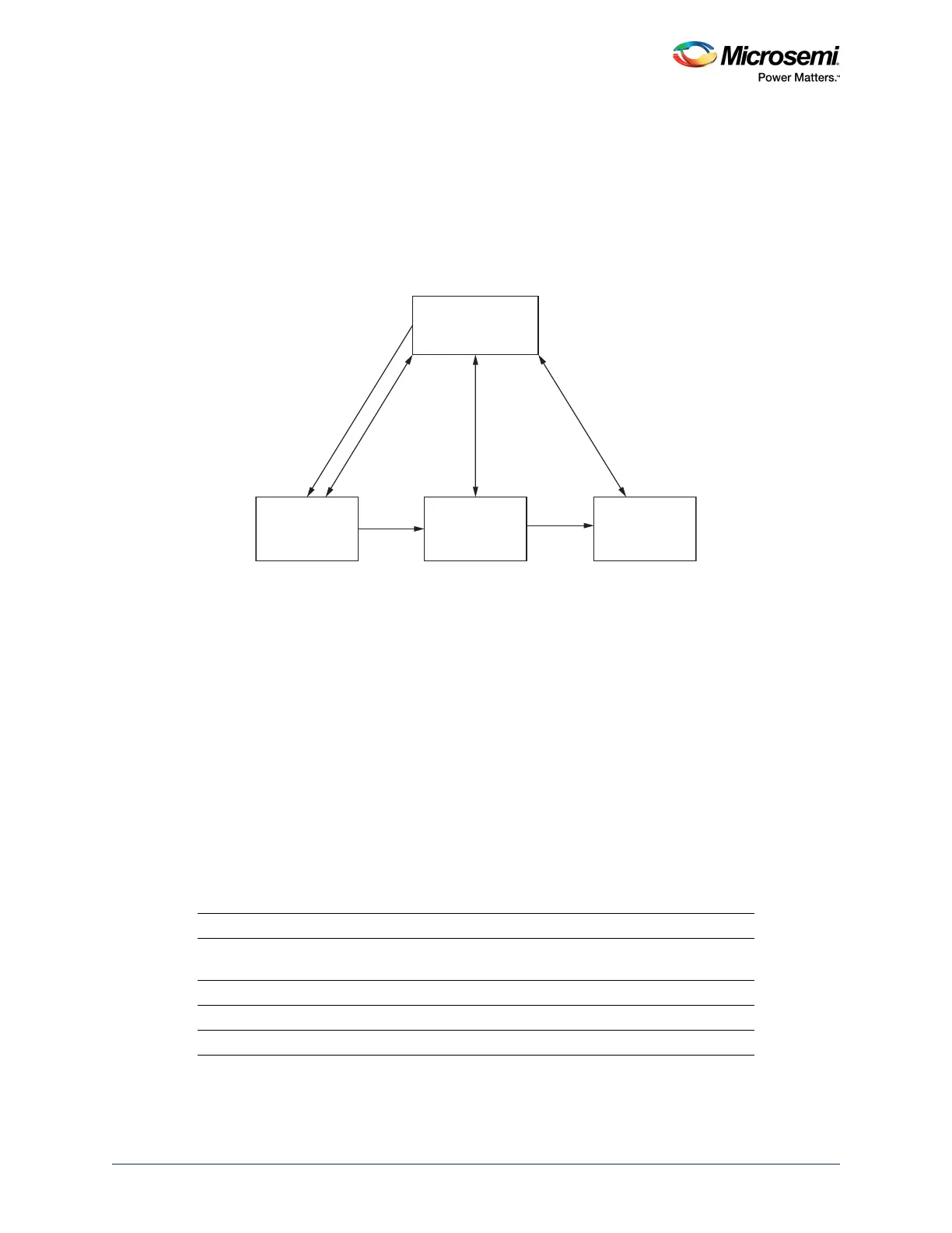
It is required to ensure that the placement for the DDR3 memories looks like L (shape), where, memories
are at the bottom of the L and controllers are on the top of the L. This gives enough space to route the
DQ signals with less number of layers. This is not mandatory to follow the suggested placement.
However, the placement also depends on the board constraints. The maximum trace length of any signal
in the placement should not be more than 7 inches.
Figure 61 • DDR3 Memories
The termination resistors are not required for the DQ and DQS signals as these signals have on chip
ODTs. The termination resistors are placed at the end of the address, command, control, and clock
signals as these signals use fly-by topology. VTT plane/island is thick enough to handle the current
required by termination resistors; at least 150 mil trace is required. The sense pin of VTT regulator
should be connected at the center of the VTT island.
3.10.2 Routing
Reliability of DDR interface depends on the quality of the layout. There are many layout guidelines
available from memory vendors. The following recommendations can also be used for routing the DDR3
signals. The following DDR3 signals are grouped:
• Data
• Address/Command
• Control
• Clocks
• Power
The following table lists the signals that come under a particular group:
Table 22 • Grouping of DDR3 Signals
Group Signals
Data DQ[0:7], DQ[8:15], DQ[16:23], DQ[24:31] and DQS[0:3],
DM[0:3]
Address/Command A[0:15], BA[0:2], RAS#, CAS#, and WE#
Control CS#, CKE, and ODT
Clock CK and CK#
SmartFusion2
DDR3 DDR3 DDR3
Address/Control/Command/Clock Routing
Data[0:7]
Data[8:15]
Data[16:23]