Layout Guidelines for SmartFusion2- and IGLOO2-Based Board Design
AC393 Application Note Revision 14.0 52
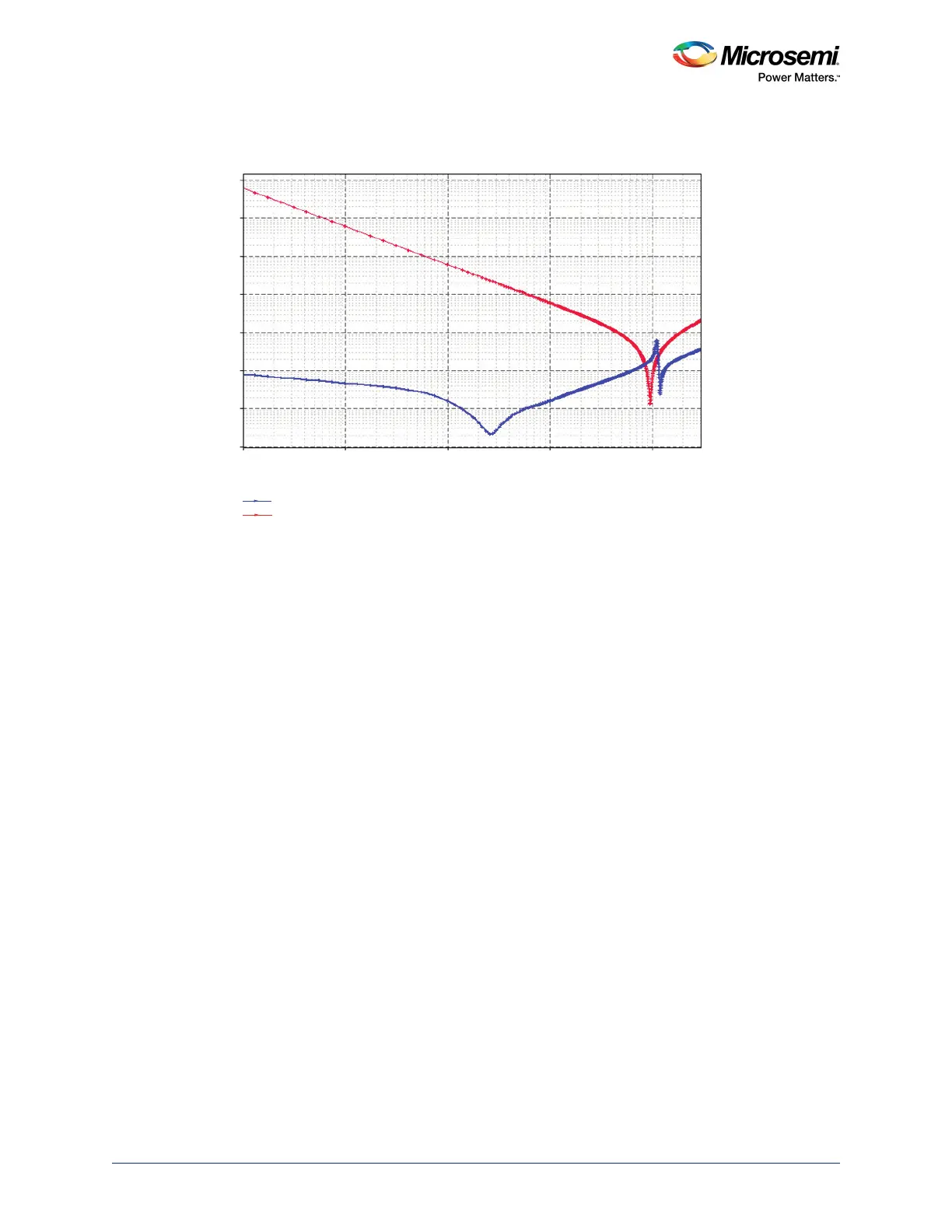
Figure 43 • PLL0VDDA Plane Impedance
3.6 I/O Power Supply
3.6.1 Component Placement
• The bypass capacitors (47 µF and 22 µF) should be placed near, or if possible, at the edge of the
device.
• All decoupling capacitors (0.1 µF and 0.01 µF) should be 0402 or of a smaller package size as they
are required to be mounted under BGA package. They should be fit between the adjacent vias of
BGA package pins. These decoupling capacitors are selected to have a low impedance over
operating frequency and temperature range.
The capacitor pad to via trace should be as small as possible. Figure 24, page 39 shows how these
capacitors are mounted. The capacitors can also be mounted directly on the pad available on the vias.
The decoupling capacitors should not be shared via connections.
3.6.2 Plane Layout
The shape of the plane does not have a specific requirement. The width of the plane should be sufficient
enough to carry the required current.
Z Amplitude (Ω)
Frequency (GHz)
PLL0VDDA impedance with Filter Capacitors
PLL0VDDA impedance without Filter Capacitors
1e3
1e4
1e5
100
10
1
0.1
1e-4 2e-4 1e-3 2e-3 0.01 0.02 0.1 0.2 0.3 1 2 3
0.01