Board Design Guidelines for SmartFusion2 SoC and IGLOO2 FPGAs
AC393 Application Note Revision 14.0 25
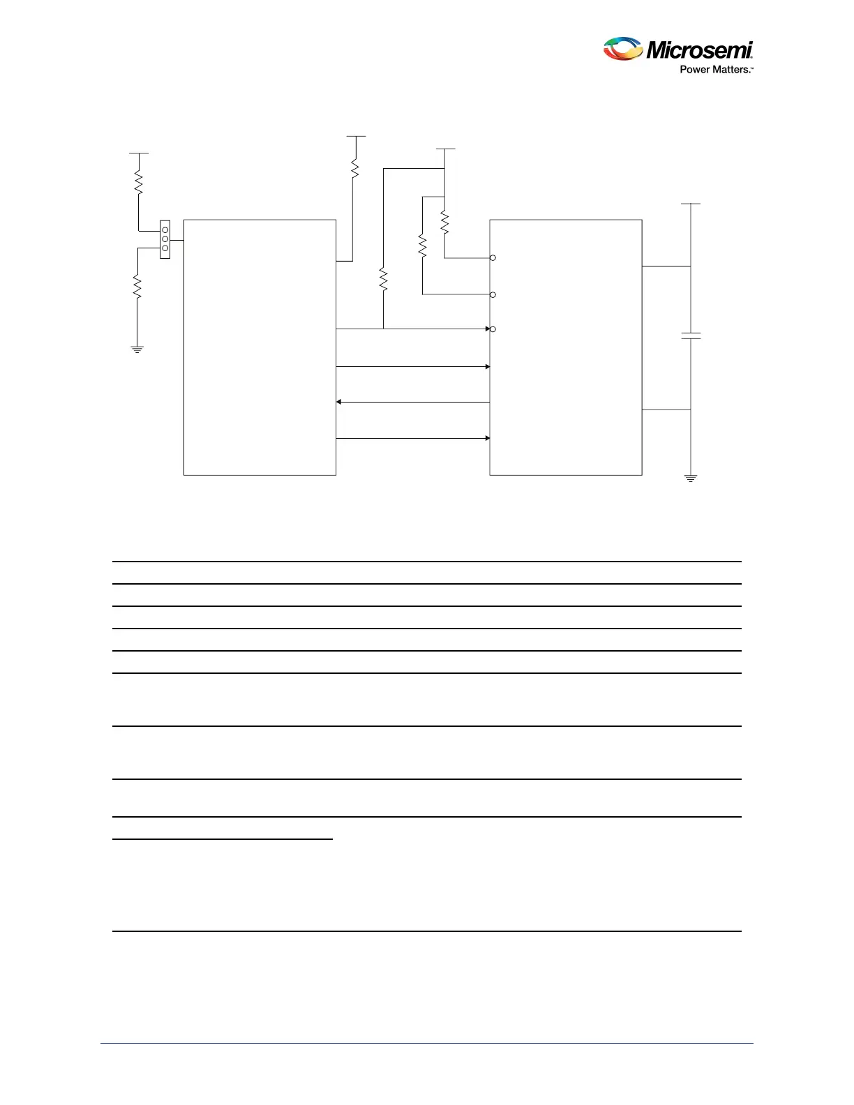
Figure 12 • SPI Master Mode Programming
The following table lists the dedicated pins used for programming the device and probing the fabric I/O.
1. Active Low Signal.
For more information about programming, see UG0451: SmartFusion2 and IGLOO2 Programming User
Guide.
Table 16 • Dedicated Pins
Special Pins Direction Description
SPI_0_SDI Input Serial data input
SPI_0_SDO Output Serial data output
SPI_0_CLK Output Serial clock. It is a serial programmable bit rate clock out signal.
SPI_0_SSO
1
Output Slave select
FLASH_GOLDEN_N
1
Input If pulled low, the SPI_0 port is put into master mode, which indicates that
the device is to be reprogrammed from an image in the external SPI flash
attached to the SPI_0 interface.
NC No connect. Indicates the pin is not connected to circuitry within the
device. NC pins can be driven to any voltage or can be left floating with
no effect on the operation of the device.
DNC Do not connect. Must not be connected to any signals on the PCB. DNC
pins must be left unconnected.
PROBE_A The two live probe I/O pins are dual-purpose:
- Live probe functionality
- User I/O
The unused live probe I/Os can be configured as weak pull-up resistors,
and these pins can be connected to the 10 kΩ external resistor. The 10
kΩ external resistor power supply must be the same as the I/O bank
power supply (VDDI).
PROBE_B
VDDIOy
3 Pin Jumper
10 K
10 K
10 K
10 K
10 K
3.3 V
3.3 V
0.1
µ
F
VPP
FLASH_GOLDEN_N
DEVRST_N
SPI_0_SDI
SPI_0_SDO
VCC
External Flash
SmartFusion2/IGLOO2
(Master)
DI
DO
GND
CLK
CS
HOLD
WP
SPI_0_CLK
SPI_0_SS0
y=bank number where
this pin is located
10 K