Layout Guidelines for SmartFusion2- and IGLOO2-Based Board Design
AC393 Application Note Revision 14.0 56
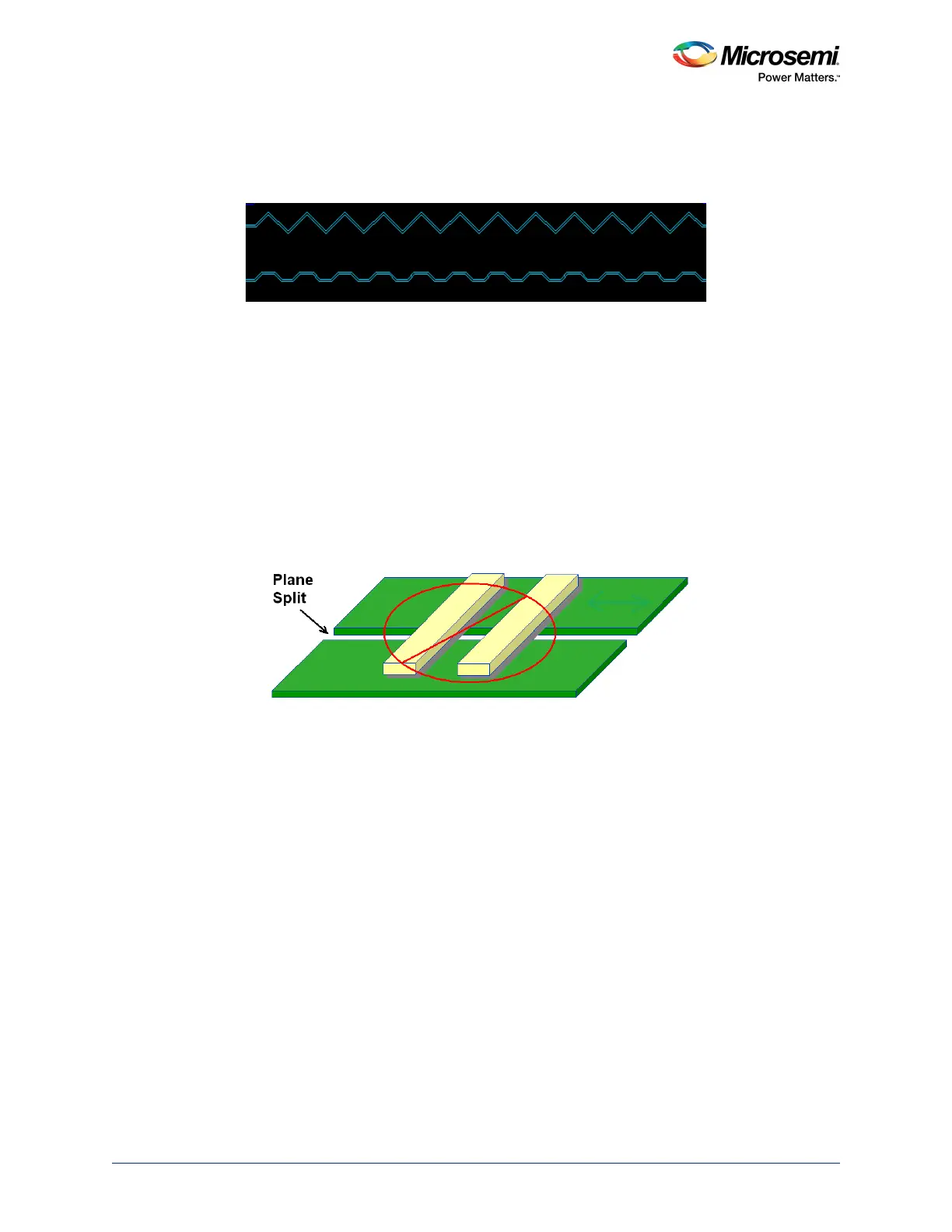
• 2116 or 2113 glass weaving PCB materials should be used to avoid the variations in the
impedances. Zig-zag routing must be used instead of straight line routing to avoid glass
weaving effect on impedance variations, as shown in the following figure. Instruct the fabrication
vendor to use these PCB materials before manufacturing.
Figure 49 • Zig-Zag Routing
• These traces should be kept away from the aggressive nets or clock traces. For example, on
M2S050T devices, the SerDes and DDR traces should not be adjacent to each other.
• Separation between the coupled differential trace pairs should be 1x. Spacing between
channels should be > 3x separation. Trace stubs should be avoided. The stub length should not
exceed 40 mils for 5 Gbps data rate.
• The trace lengths should be kept as small as possible.
• It is better to use low roughness, that is, smooth copper. As the speed increases insertion loss
due to the copper, then roughness increases. The attenuation due to skin effect is increased
proportional to the square root of frequency. The roughness courses this loss proportional to
frequency. Microsemi recommends instructing the PCB fabrication house to use smooth copper,
if the frequency exceeds 2 Gbps.
• Split reference planes should be avoided. Ground planes must be used for reference for all the
SerDes lanes.
Figure 50 • Ground Planes for Reference
3.8.2 Via
• The target impedance of vias are designed by adjusting the pad clearance (anti-pad size). Field
solver should be used to optimize the via according to the stack-up.