Board Design Guidelines for SmartFusion2 SoC and IGLOO2 FPGAs
AC393 Application Note Revision 14.0 34
2.10 User I/O and Clock Pins
The following table lists recommendations for unused I/O and clock pins in a SmartFusion2/IGLOO2
device.
2.10.1 Internal Clamp Diode Circuitry
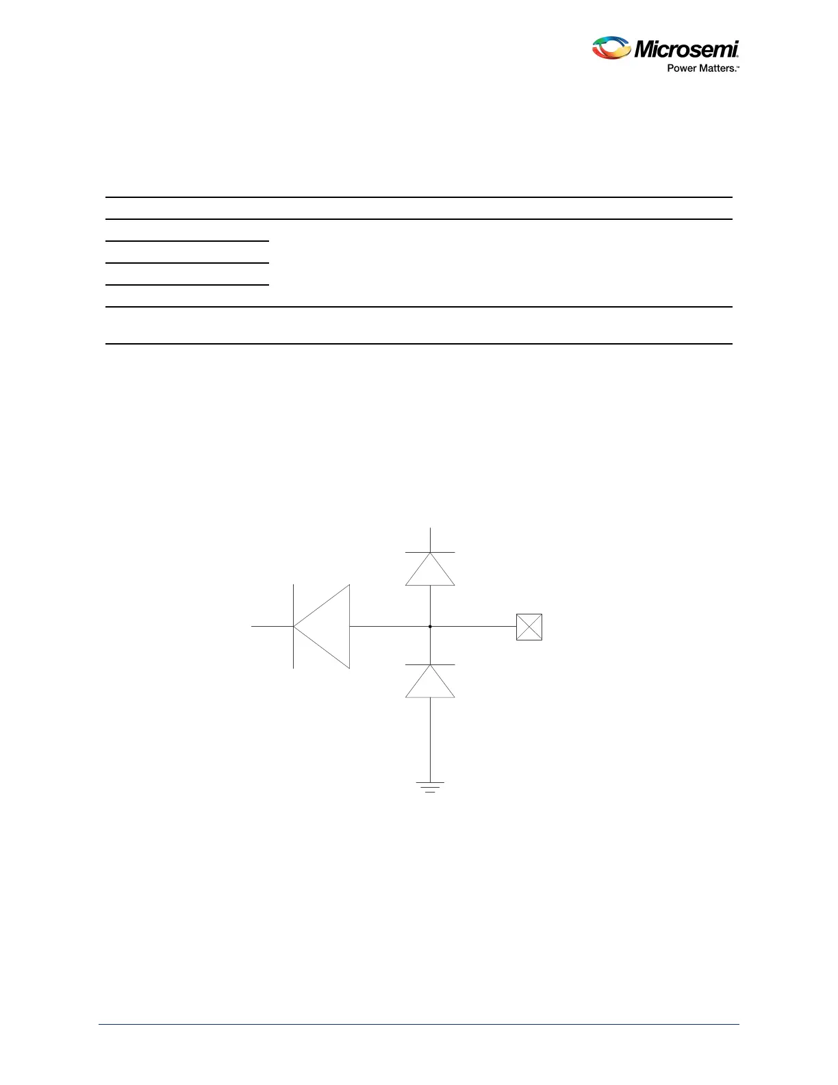
All user I/Os have an internal clamp diode control circuitry, as shown in the following figure. A pull-up
clamp diode must not be present in the I/O circuitry if the hot-swap feature is used. The 3.3 V PCI
standard requires a pull-up clamp diode and, therefore, cannot be selected if hot-swap capability is
required.
Figure 21 • Internal Clamp Diode Control Circuitry
For more information about hot swapping and cold sparing applications, see the AC396: SmartFusion2
and IGLOO2 in Hot Swapping and Cold Sparing Application Note
.
Table 18 • Recommendations for Unused I/O and Clock Pins
I/O Unused Condition Remarks
MSIO Libero-Defined DNC
1
1. Libero configures unused user I/O (MSIO, MSIOD, and DDRIO) as: input buffer disabled, output buffer tristated with weak
pull-up.
Internal weak pull-up is available
MSIOD
DDRIO
Programming SPI pins
Crystal oscillator pins Must be left floating and must not
connect to ground (VSS)
Internal weak nominal 50 kΩ pull-up to VPP
Buffer
Pad
VDDI
Pull-up clamp diode
present in 3.3 V PCI,
MSIO, MSIOD, and
DDRIOs
Pull-down clamp diode
present in all user I/O
standards