Layout Guidelines for SmartFusion2- and IGLOO2-Based Board Design
AC393 Application Note Revision 14.0 39
Subsequent sections display simulation results based on target impedance calculated using preceding
equation. Microsemi strongly recommends calculating the target impedance and performing simulations
for the impedance profile of the power plane. These simulations help in optimizing the decoupling
capacitors to reduce the production cost and have the optimal placement. The plane shapes given in this
document are with reference to the UG0557: SmartFusion2 SoC FPGA Advanced Development Kit User
Guide. This may vary depending on the design. For simulation topology, see Appendix: Power Integrity
Simulation Topology, page 94.
SmartFusion2/IGLOO2 power supplies are classified as:
• Core power supply
• I/O power supply
• Serializer/deserializer (SerDes) power supply
• Double data rate (DDR) power supply
• Phase-locked loop (PLL) power supply
3.2 Core Supply (VDD)
The core power supply must have a low-noise and low-ripple voltages, as per datasheet. Proper care
should be taken while designing the power supply (VDD) for core. Proper placement of decoupling
capacitors and plane geometry greatly influences the power supply distribution going into
SmartFusion2/IGLOO2 device.
3.2.1 Component Placement
• The bulk capacitors (330 µF and 100 µF) should be placed near by the SmartFusion2/IGLOO2
device.
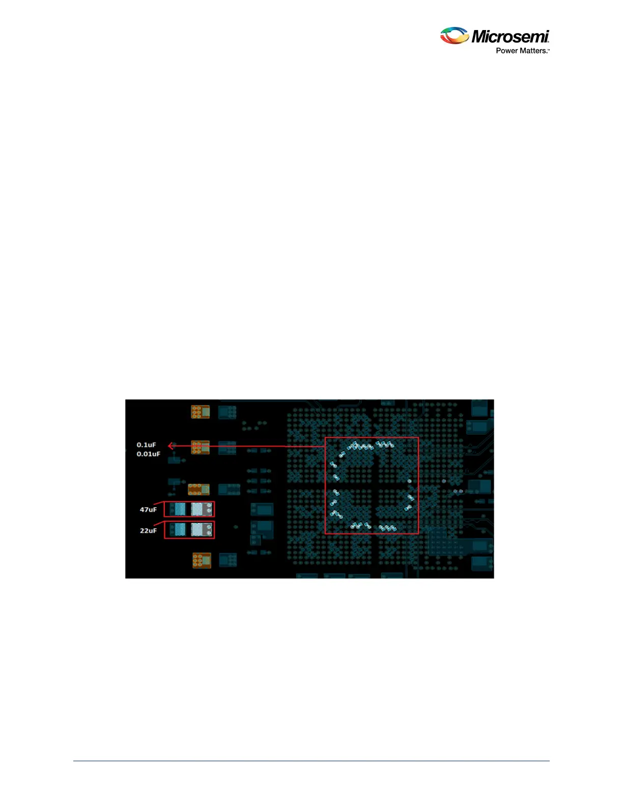
• The bypass capacitors (47 µF and 22 µF) should be placed near or if possible, on the periphery of
the device. The placement on the SmartFusion2 Development Kit board is shown in the following
figure.
Figure 24 • Placement of Capacitors for VDD Plane
• All decoupling capacitors (0.1 µF and 0.01 µF) should be 0402 or of a smaller package size, as they
are required to be mounted on the back side of the board. They should be fit between the adjacent
vias of ball grid array (BGA) package pins. These decoupling capacitors are selected to have a low
impedance over operating frequency and temperature range. Capacitor pad to via trace should be
as small as possible. The following figure shows how these capacitors need to be mounted.
Microsemi recommends keeping the capacitor pad directly on the corresponding vias. The
capacitors should not share ground vias. Each decoupling capacitor should have its own via
connection to the PCB ground plane.
• The De-coupling capacitor and the Smart Fusion2\IGOOL2 device can be placed side by side. If
placed side by side, route the power with thick traces. Microsemi does not guarantee on noise on
power rails. User must run the power simulation.
 Loading...