Layout Guidelines for SmartFusion2- and IGLOO2-Based Board Design
AC393 Application Note Revision 14.0 51
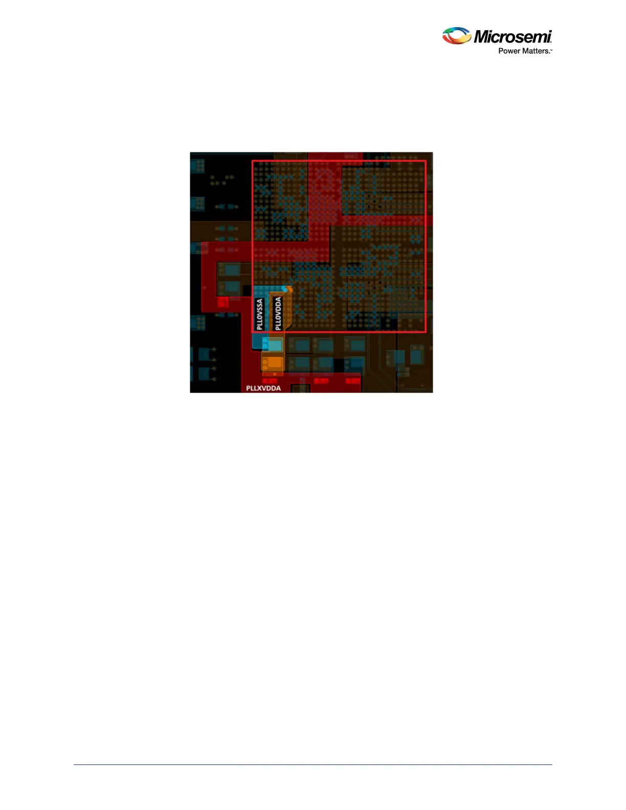
3.5.2 Plane Layout
• Plane routing for PLL0VDDA and PLL0VSSA is shown in the following figure. These are with respect
to the schematic, as shown in Figure 40, page 50.
• The capacitor (22 µF) and series resistor should be placed near the device as close as possible to
the 0.1 µF cap. A sample placement is shown in the following figure.
Figure 42 • Routing for PLL Filter Circuit
• PLL0VDDA and PLL0VSSA should not be routed with a small trace width as it increases the
inductance resulting in ripples. These supply traces should be routed as plane (as shown in
Figure 42, page 51), even though the current requirements are small.
• Same layout guidelines should be followed for DDR PLL power supplies. For more information about
PCIe PLL guidelines, see SerDes, page 41.
3.5.3 Simulations
The target impedance of the PLL0VDDA plane is calculated as 16.5 Ω based on the values (see Power
Supply, page 38):
•V
SUPPLY
= 3.3 V
• 3.3 V, I
trans
= 10 mA
• Ripple = 5%
The impedance of the place (Z) should be 16.5
Ω or less. For more information about ripples and its
values, see DS0128: IGLOO2 and SmartFusion2 Datasheet. Plane impedance with and without filter
circuit is shown in Figure 43, page 52.
 Loading...