Layout Guidelines for SmartFusion2- and IGLOO2-Based Board Design
AC393 Application Note Revision 14.0 40
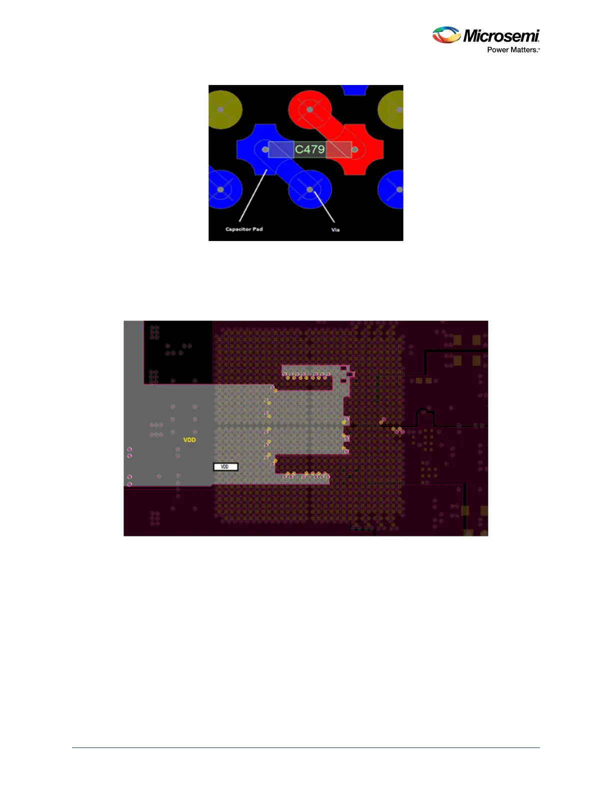
Figure 25 • Capacitor Placement under BGA Vias
3.2.2 Plane Layout
Microsemi recommends using the VDD plane, as shown in the following figure.
Note: The plane can be routed in multiple ways. The goal is to have a dedicated and low-impedance plane.
Figure 26 • VDD Plane
3.2.3 Simulations
The effect of the decoupling capacitors can be visualized through the power integrity simulations. The
target impedance of the VDD is calculated as 40 m
Ω, based on the following values:
•V
SUPPLY
= 1.2 V
•I
trans
= 1.5 A
• Ripple = 5%
Figure 27, page 41 shows the impedance profile of the VDD plane of the SmartFusion2 Development Kit.
It shows that the capacitors used are adequate to improve the impedance profile over the bandwidth.
Good coupling between the planes can be achieved by having power and ground plane in adjacent
layers. Once all the capacitors (0.1 µF and 0.01 µF) are placed, the impedance of the VDD plane
impedance profile improves over the frequency range. The simulation results shown in this document are
done in Sigrity PowerSI tool. For more information on how to do the simulation, see the Sigrity PowerSI
Tutorial.
 Loading...