Layout Guidelines for SmartFusion2- and IGLOO2-Based Board Design
AC393 Application Note Revision 14.0 57
Figure 51 • Via Illustration
1
• Number of vias on different traces should be avoided or minimized. SerDes signals should be routed
completely on a single layer with the exception of via transitions from component layer to the routing
layer (3-via maximum).
• The length of via stub should be minimized by back drilling the vias, or by routing the signals from
near top to near bottom layer, or else blind or buried vias can be used. Using blind-vias or back
drilling is a good method to eliminate via stubs and reduce reflections.
• The stub length should be kept below 100 mils, if the data rate is 2.5 Gbps and 40 mils for
5 Gbps.
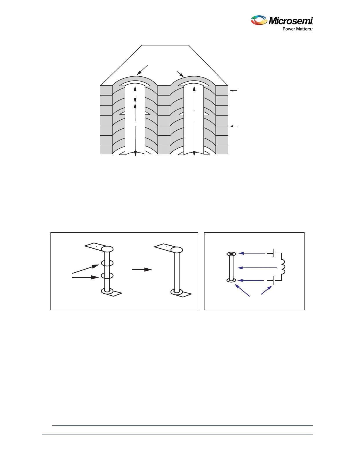
• If feasible, non-functional pads should be removed. Non-functional pads on via are the pads where
no trace is connected. This reduces the via capacitance and stub effect of pads.
Figure 52 • Non-Functional Pads of Via
• The tight via to via pitch is practical to reduce the cross talk effect, as shown in the following figure.
1. Simonovich, E. Bogatin, Y. Cao, Method of Modeling Differential Vias, White Paper, Jan 2011
Anti-Pad
Pad
Stub
Via
Via
Barrel
Dielectric
Typ.
Copper
Planes
Typ.
Unused
Pad
Via
Circuit
Model
Changing Pad and Anti-Pad
diameter changes capacitance