Layout Guidelines for SmartFusion2- and IGLOO2-Based Board Design
AC393 Application Note Revision 14.0 42
3.3.1.3 SerDes PLL
There are two power supply nodes required for SerDes. One is SERDES_x_VDDAPLL and another is
SERDES_x_PLL_VDDA. Both of these supplies require separate filter circuits. Filter circuit for
SERDES_x_VDDAPLL is shown in the following figure. A typical filter circuit for SERDES_x_PLL_VDDA
is shown in the following figure.
Figure 28 • Filter Circuit for SerDes PLL Power Supply
• C1 and R1 should be placed near the device.
• C2 should to be placed under the BGA via. The capacitor pad to via trace should be as small as
possible.
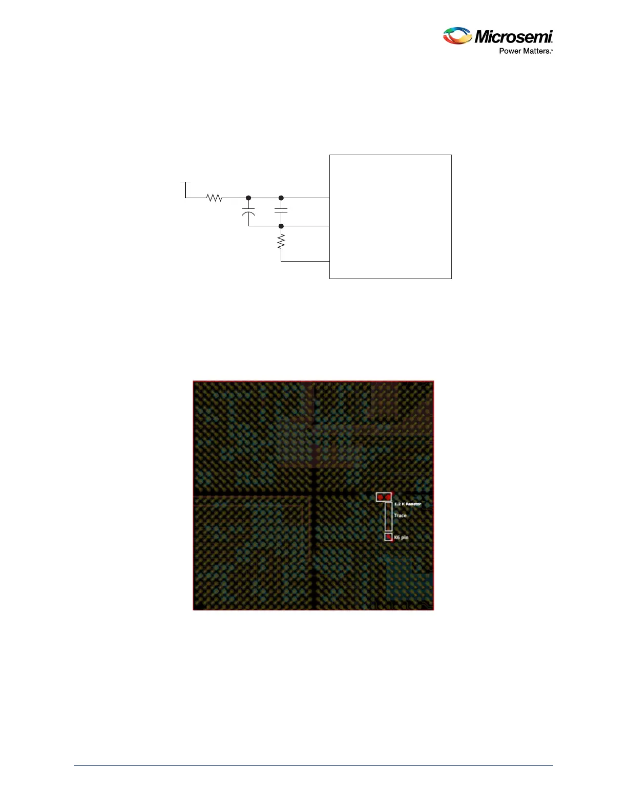
• Apart from this, a precision resistor (1.2 K) is placed between the SERDES_x_REXT and
SERDES_x_REFRET pins. This resistor should be placed near the BGA via of SERDES_x_REXT
pin. Any aggressive signal traces should be kept away from this resistor to avoid unwanted noise
from coupling into this critical circuit. A sample placement is shown in the following figure.
Figure 29 • Component Between 1.2 K Resistor and K6 Pin
For more information about R1, C1, and C2, see Board Design Guidelines for SmartFusion2 SoC and
IGLOO2 FPGAs, page 4.
+2.5 V
R1
C1
C2
1.2K_1%
SERDES_x_REFRET
SERDES_x_REXT
SERDES_x_VDDAPLL
SmartFusion2
 Loading...