Creating Schematic Symbols Using Cadence OrCAD Capture CIS for SmartFusion2
and IGLOO2 Designs
AC393 Application Note Revision 14.0 69
4 Creating Schematic Symbols Using Cadence
OrCAD Capture CIS for SmartFusion2 and
IGLOO2 Designs
Creating symbols manually for application can be a time consuming task and is error prone. Cadence
OrCAD Capture is a popular schematic design entry tool for system-level design.
This application note describes the recommended procedure to create schematic symbols. The
schematic symbols can be created using two methods:
• Using the Microsemi published pin assignment tables (PAT) in spreadsheet format. Pin Information
is imported into OrCAD Capture CIS tool. This is a two step process as explained in Creating
Schematic Symbols using Pin Assignment Tables (PAT), page 69. Use this method for creating
schematic symbols using Microsemi defined pins.
• Using the data export feature of Libero SoC software. Pin information can be exported to a
spreadsheet and then use OrCAD Design Capture CIS tool to create symbols. This is a three step
process as explained in Creating Schematic Symbols with User Defined Pin Names, page 76. Use
this method for creating symbols using user defined pins for the fabric I/Os.
4.1 Creating Schematic Symbols using Pin Assignment
Tables (PAT)
4.1.1 Preparing the PAT Layout File for Import into OrCAD Capture
1. Download the PAT files from the following path in the Microsemi website under Datasheets section:
• www.microsemi.com/products/fpga-soc/soc-fpga/smartfusion2#documents
• www.microsemi.com/products/fpga-soc/fpga/igloo2-fpga#documents
2. Open the *Pin_Assignment_Table_Public.xlsx file.
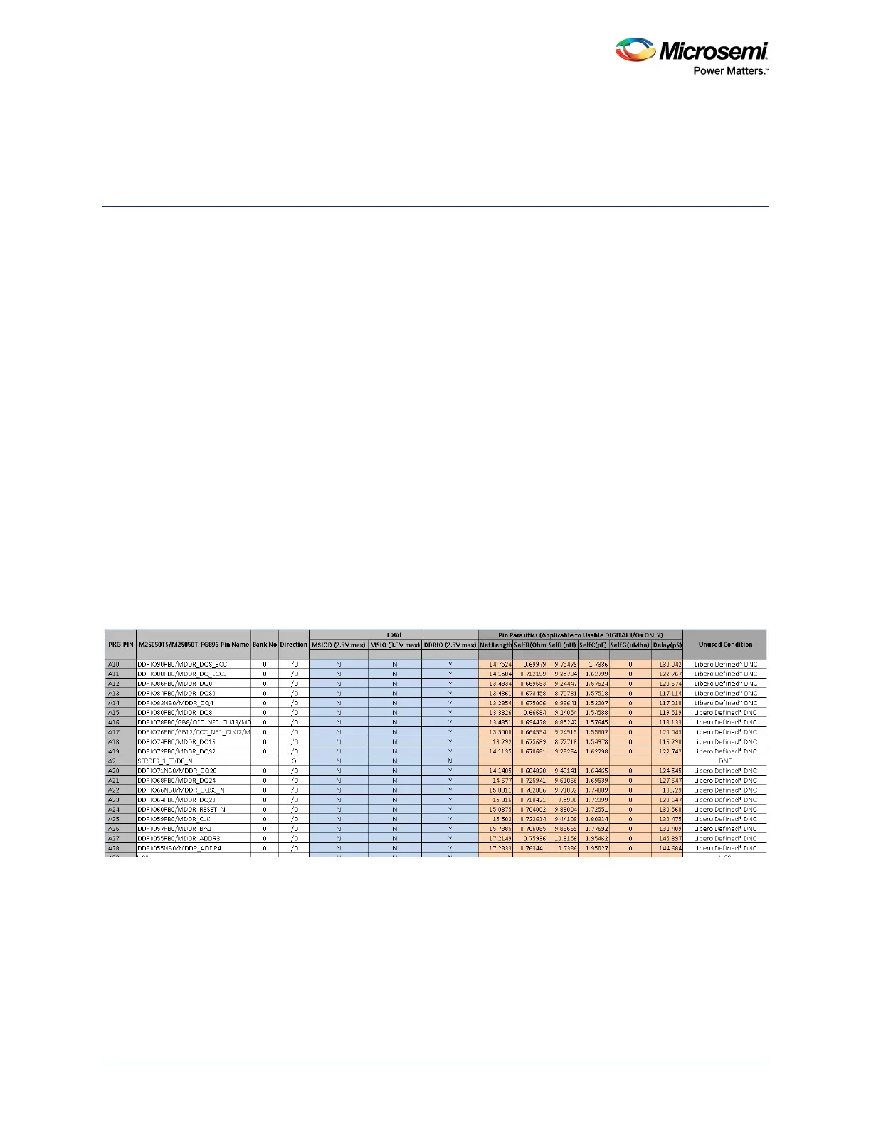
Figure 67 • Example PAT Spreadsheet - Initial view
3. Go to the sheet that has the device name that you require.
4. Retain the following columns and delete the remaining columns:
• PGK.PIN
• <Device> Pin Name
• Direction
5. Insert a row at the beginning of the worksheet. See Figure 68, page 70.
 Loading...