53
Rev. 2.0
07/27/2023
MBDV Hardware Manual
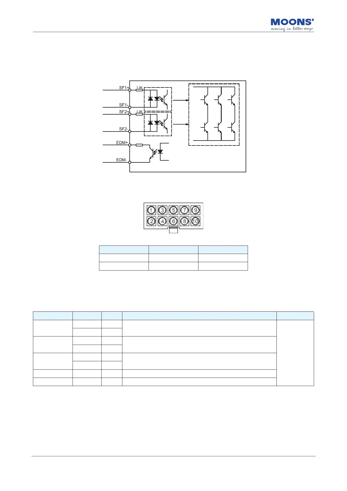
4.11.2 STO Function Connector
4.11.2.1 STO Internal Circuit Diagram
The pinout of the STO connector is as follows:
4.11.2.2 STO Signal Denitions
The pin denition of driver CN5 is as follows:
Connector and terminal models are as follows:
Model manufacturer
Connector 43025-1000 MOLEX
PIN 43030-0005 MOLEX
4.11.2.3 STO Signal Denitions
STO function input and output signals are as follows
Signal name Logo Pin Description Applicable mode
Safety signal
input 1
SF1+ 1
When the SF1 signal is removed, that is, SF1 is o, the STO
function is activated (enabled).
All control
modes
SF1- 5
Safety signal
input 2
SF2+ 3
When the SF2 signal is removed, that is, SF2 is o, the STO
function is activated (enabled).
SF2- 2
Safety signal
output
EDM+ 6
When the STO function works, this signal is output
EDM- 4
Digital Ground DGND 7,8 +5VDC power ground
+5V +5V 9,10 +5VDC power source
Note: When any safety input SF1 and SF2 are OFF, the STO function will start to work.