11. Timer 0/1/2 A96G166/A96A166/A96S166 User’s manual
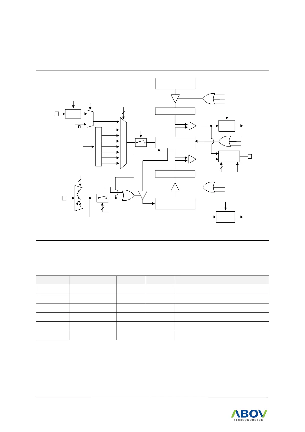
11.3.4 16-bit timer 2 block diagram
In this section, a 16-bit timer 2 is described in a block diagram.
T2MS[1:0]
T2POL
Reload
A Match
T2CC
T2EN
P
r
e
s
c
a
l
e
r
fx
M
U
X
fx/2
fx/4
fx/64
fx/512
fx/2048
fx/8
fx/1
Comparator
16-bit Counter
T2CNTH/T2CNTL
16-bit B Data Register
T2BDRH/T2BDRL
Clear
B Match
Buffer Register B
Comparator
16-bit A Data Register
T2ADRH/T2ADRL
T2IFR
INT_ACK
Clear
To interrupt
block
A Match
Buffer Register A
Reload
Pulse
Generator
T2O/
PWM2O
R
EINT12
T2CNTR
T2EN
3
T2CK[2:0]
Clear
EIPOL1[5:4]
FLAG12
(EIFLAG1.6)
INT_ACK
Clear
To interrupt
block
2
2
T2MS[1:0]
2
T1 A Match
A Match
T2CC
T2EN
A Match
T2CC
T2EN
M
U
X
Edge
Detector
EC2
T2ECE
T2ECS
NOTE: T1 A Match is a pulse for the timer 2 clock source if it is selected.
Figure 56. 16-bit Timer 2 Block Diagram
11.3.5 Register map
Table 20. TIMER 2 Register Map
Timer 2 A Data High Register
Timer 2 A Data Low Register
Timer 2 B Data High Register
Timer 2 B Data Low Register
Timer 2 Control High Register
Timer 2 Control Low Register