22. Development tools A96G166/A96A166/A96S166 User’s manual
22.5 On-chip debug system
A96G166/A96A166/A96S166 supports On-chip debug (OCD) system. We recommend to develop and
debug program with A96G1 series. On-chip debug system of A96G166/A96A166/A96S166 can be
used for programming the non-volatile memories and on-chip debugging. Detail descriptions for
programming via the OCD interface can be found in this section.
Table 65 introduces features of OCD.
Table 65. OCD Features
Two wire external interface
1 for serial clock input
1 for bi-directional serial data bus
All internal peripherals
Internal data RAM
Program Counter
Flash memory and data EEPROM memory
Extensive On-Chip Debugging
supports for Break Conditions
Break instruction
Single step break
Program memory break points on single address
Programming of Flash, EEPROM, Fuses, and Lock bits
through the two-wire interface
On-Chip Debugging supported by Dr. Choice
The maximum frequency of a target MCU.
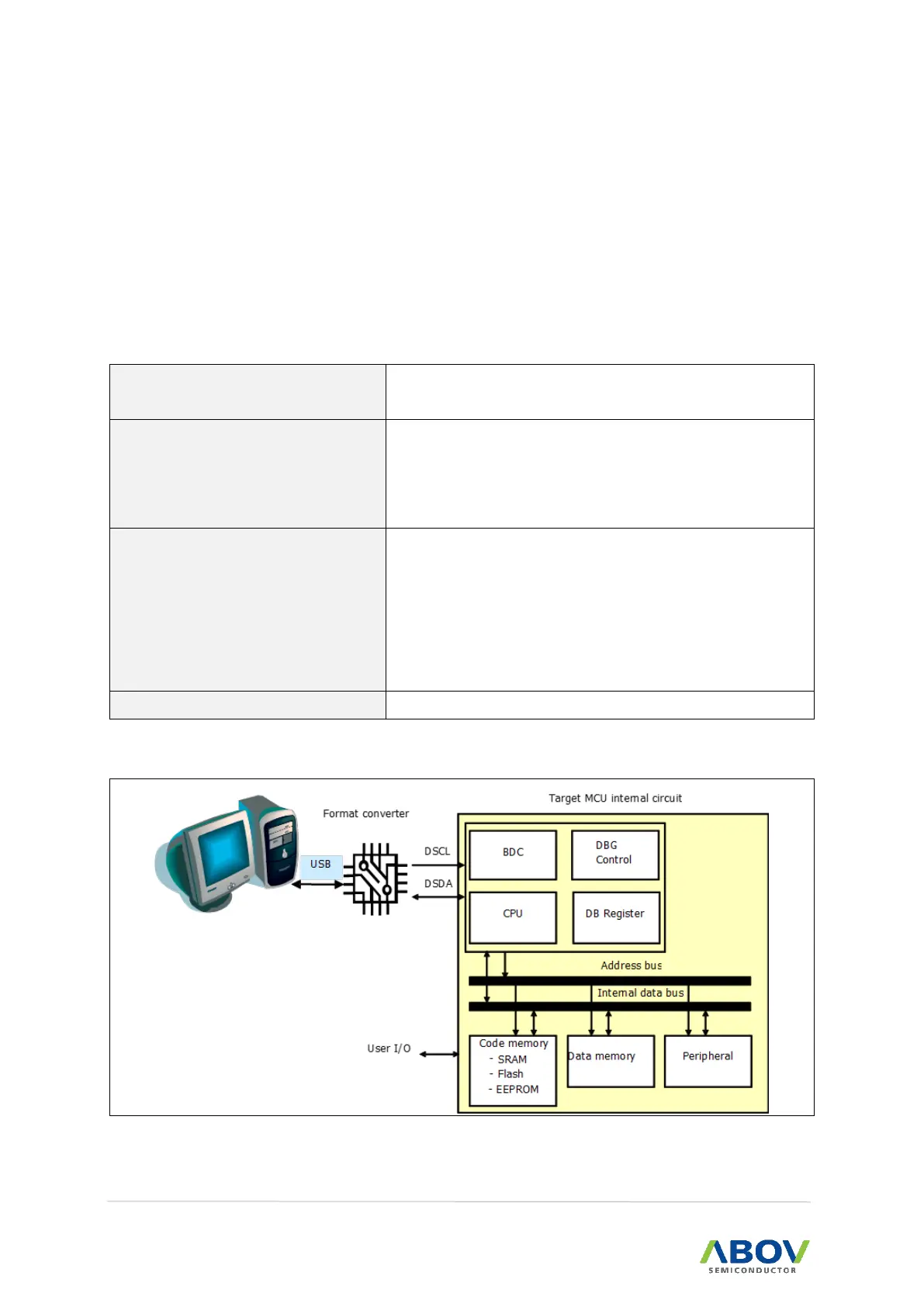
Figure 136 shows a block diagram of the OCD interface and the On-chip Debug system.
Figure 136. On-Chip Debugging System in Block Diagram