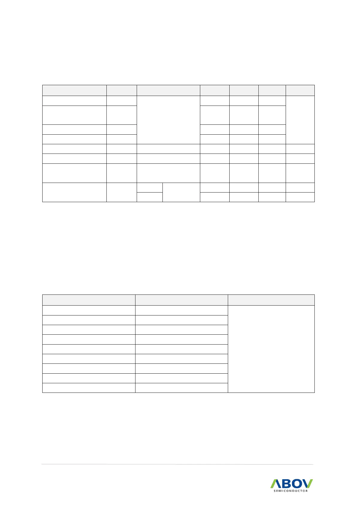
20.3 A/D converter characteristics
Table 45. A/D Converter Characteristics
(T
A
=-40°C ~ +85°C or T
A
=-40°C ~ 105°C, VDD=2.2V ~ 5.5V, VSS=0V)
NOTES:
1. When VDD is lower than 2.2V, the ADC resolution will get worse.
2. Zero offset error is the difference between 000000000000 and the converted output for zero input
voltage (VSS).
3. Full scale error is the difference between 111111111111 and the converted output for full-scale input
voltage (VDD).
4. If VDD is less than or equal to 2.2V, the resolution degrades by 1-bit whenever VDD drops 0.1V.
(@ADCLK = 0.5MHz, under 2.2V, resolution has no test.)
5. ADCLK must be less than 0.5MHz. Furthermore, if ADCLK is less than 0.125MHz, it can be improved
INL characteristic.
Table 46. Recommended ADC Resolution
(T
A
=-40°C ~ +85°C or T
A
=-40°C ~ 105°C, VDD=2.5V ~ 5.5V, VSS=0V)