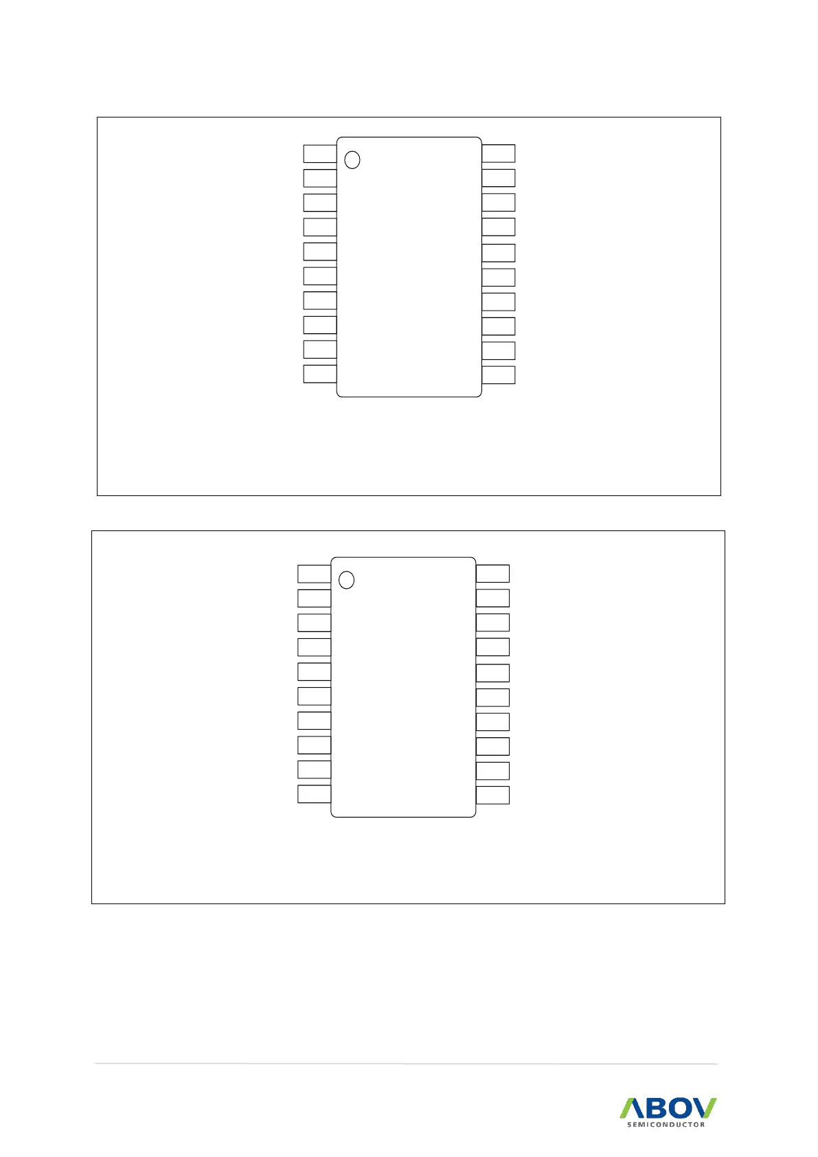
2. Pinouts and pin description A96G166/A96A166/A96S166 User’s manual
A96G166FR
(20TSSOP)
A96G166FD
(20SOP)
1
4
3
2
VSS
6
5
VDD
7
10
9
8
20
17
18
19
15
16
14
11
12
13
P37/XOUT
P35/EINT10/T0O/PWM0O
P36/XIN
P32/(T0O)/(PWM0O)/RESETB
P31/(EC0)/RXD1/(SCL)
P30/(EC2)/TXD1/(SDA)
P25/SCL/(RXD1)
P24/SDA/(TXD1)
P22/EINT9/XCK1/LED6
P00/AN0/DSDA
P01/AN1/DSCL
P02/AN2/EINT0
P03/AN3/EINT1/(T1O)/(PWM1O)
P10/AN7/EINT5/PWM1OB
P11/AN8/EINT6/EC1/BUZO
P12/AN9/EINT11/T1O/PWM1O/LED0
P13/AN10/EINT12/T2O/PWM2O/LED1
P21/EINT8/SS1/LED5
NOTES:
1. The programmer (E-PGM+, E-Gang4/6) uses P0[1:0] pin as DSCL, DSDA.
2. The P04-P06, P14-P17, P20, P23, P26 and P33-P34 pins should be selected as a push-pull
output or an input with pull-up resistor by software control when the 20-pin package is used.
Figure 3. A96G166 20TSSOP/20SOP Pin Assignment
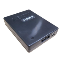
A96A166FD
(20SOP)
1
4
3
2
VSS
6
5
VDD
7
10
9
8
20
17
18
19
15
16
14
11
12
13
P37/XOUT
P35/EINT10/T0O/PWM0O
P36/XIN
P32/(T0O)/(PWM0O)/RESETB
P31/(EC0)/RXD1/(SCL)
P30/(EC2)/TXD1/(SDA)
P25/SCL/(RXD1)
P24/SDA/(TXD1)
P15/AN12/TXD0
P00/AN0/DSDA
P01/AN1/DSCL
P02/AN2/EINT0
P03/AN3/EINT1/(T1O)/(PWM1O)
P10/AN7/EINT5/PWM1OB
P11/AN8/EINT6/EC1/BUZO
P12/AN9/EINT11/T1O/PWM1O/LED0
P13/AN10/EINT12/T2O/PWM2O/LED1
P14/AN11/RXD0
NOTES:
1. The programmer (E-PGM+, E-Gang4/6) uses P0[1:0] pin as DSCL, DSDA.
2. The P04-P06, P16-P17, P20-P23, P26 and P33-P34 pins should be selected as a push-pull output or
an input with pull-up resistor by software control when the 20-pin package is used.
Figure 4 A96A166 20SOP Pin Assignment