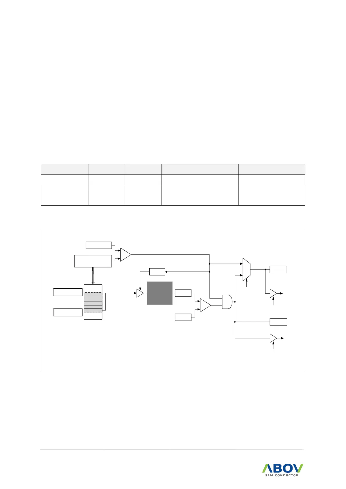
EasyManua.ls Logo

Abov A96G166 User Manual

Default Icon
247 pages
To Next Page IconTo Next Page
To Previous Page IconTo Previous Page
Page #162 background imageLoading...
Page #162 background image
16. CRC A96G166/A96A166/A96S166 User’s manual
162
16 CRC
Using the CRC, it can be monitor the memory of the specified area. This is a one-time operation, and
reset is required for continuous operation. In CRC MNT mode, when the CRC read is finished,
CRC_FLAG occurs. In CRC validate mode, if the CRC validate fail after the CRC reading is finished,
CRC_FLAG occurs. CRC_FAIL indicates the status of validate results when the CRC read is finished.
If the CRC_FLAG is generated and the interrupt is enabled, interrupt service routine is served. CRC-
FLAG is not cleared by hardware. CRC-TYPE 0~3 are not supported. Validate is done by comparing
the CRC_MNT register and the CRC register value. CRC are not automatically initialized, you need to
calculate a new CRC after CRC_H, CRC_L Clear.
Table 30. CRC mode
CRC TYPE
CRC mode
CRC input
Condition of CRC_FLAG
Condition of CRC reset
CRC_TYPE = 4
MNT
Flash Data
After CRC reading
-
CRC_TYPE = 6
Validate
Flash Data
After CRC reading &
Validate fail
Validate fail
16.1 Block Diagram
CRC_TYPE[2:0]
FLASH
CRC calculator
CRC_MNT
CRC_ADDR_START
CRC_ADDR_END
CRC
< FLASH >
CRC_FAIL
CRC Reset
RESET_EN
CRC_FLAG
CRC Interrupt
INT_EN
After CRC reading
CRC_EN
Clear CRC_EN
Match
...
ADDR_Counter
(CRC_ADDR_START ++)
CRC_ADDR_END
Match
4
6
Figure 81. CRC Block Diagram

Table of Contents

Question and Answer IconNeed help?

Do you have a question about the Abov A96G166 and is the answer not in the manual?

Abov A96G166 Specifications

General IconGeneral
Operating Frequency48MHz
Flash Memory128KB
SRAM16KB
GPIO PortsUp to 51
Communication InterfacesUART, SPI, I2C
Operating Voltage2.0V ~ 3.6V
Operating Temperature-40°C to +85°C

Summary

Introduction

Reference document

Lists other documents and resources relevant to the product.

1 Description

1.1 Device overview

Details the core features and peripheral counts of the device.

2 Pinouts and pin description

2.1 Pinouts

Illustrates the pin configuration for various package types.

2.2 Pin description

Lists and explains the function of each pin for different packages.

3 Port structures

5.1 Port register

Details the registers controlling I/O port direction, pull-ups, and open-drain behavior.

4 Memory organization

4.1 Program memory

Describes the layout and addressing of the on-chip flash program memory.

4.2 Data memory

Details the internal RAM, SFR, and external XRAM spaces.

4.3 External data memory

Describes the XRAM and XSFR memory areas.

4.4 SFR map

Provides a summary and detailed mapping of Special Function Registers.

5 I/O ports

5.1 Port Register Details

Covers Px, PxIO, PxPU, PxOD, PxDB, PxFSR registers.

5.2-5.5 Port Descriptions

Details the P0, P1, P2, and P3 ports including their registers and function selection.

6 Interrupt controller

6.1 External interrupt

Details the configuration and operation of external interrupt pins.

6.2 Block diagram

Provides a visual representation of the interrupt controller's internal logic.

6.3 Interrupt vector table

Lists all interrupt sources, their priorities, and vector addresses.

7 Clock generator

7.1 Clock generator block diagram

Illustrates the internal structure of the clock generator.

7.2 Register map

Lists the registers used for configuring the clock generator.

8 Basic Interval Timer

8.1 BIT block diagram

Shows the block diagram of the Basic Interval Timer.

8.2 BIT register map

Lists the registers associated with the BIT.

9 Watchdog timer

9.1 Setting window open period of watchdog timer

Explains how to configure the watchdog timer's window period.

9.2 WDT block diagram

Provides a block diagram illustrating the Watchdog Timer's operation.

10 Watch timer

10.1 WT block diagram

Shows the block diagram of the Watch Timer.

10.2 Register map

Lists the registers used for controlling the Watch Timer.

11 Timer 0/1/2

11.1 Timer 0

Details the features, modes, and registers of Timer 0.

11.2 Timer 1

Details the features, modes, and registers of Timer 1.

11.3 Timer 2

Details the features, modes, and registers of Timer 2.

12 Buzzer driver

12.1 Buzzer driver block diagram

Illustrates the block diagram of the buzzer driver circuit.

13 12-bit ADC

13.1 Conversion timing

Describes the timing requirements for ADC conversion.

13.2 Block diagram

Illustrates the block diagram of the ADC module.

13.3 ADC operation

Explains the steps and flow for performing an ADC conversion.

14 I2C

14.1-14.6 I2C Bus Operations

Covers I2C block diagram, bit transfer, start/stop, data transfer, acknowledge, and arbitration.

14.7 Block Operation Details

Details I2C initialization, interrupt service, master transmitter, and slave receiver operations.

15 USART 0/1

15.1-15.6 USART Operation Basics

Covers block diagram, clocking, modes, data format, parity, and transmitter/receiver basics.

15.7-15.12 USART Advanced Features & Registers

Details receiver flags, SPI mode, RTO, and USART register descriptions.

16 CRC

16.1 Block Diagram

Shows the block diagram of the CRC module.

16.2 Register map

Lists the registers for configuring and controlling the CRC module.

17 Power down operation

17.1 Peripheral operation in IDLE/ STOP mode

Details how peripherals behave in IDLE and STOP power-down modes.

17.2 IDLE mode

Explains how to enter and exit the IDLE power-down mode.

17.3-17.4 STOP Mode Operation

Details entering STOP mode and its release conditions.

18 Reset

18.1 Reset Block Diagram and Sources

Covers reset sources, block diagram, and external reset input.

18.2-18.7 Reset Operation Details

Details POR, LVR, LVI, registers, and timing related to reset.

19 Memory programming

19.1 Flash Control and Status Registers

Covers registers for controlling and monitoring flash memory operations.

19.2 Memory Map

Describes the overall memory map, including flash memory organization.

19.3 Serial In-System Program Mode

Explains the Serial In-System Programming (ISP) method and flash operations.

19.4 Mode Entrance Method of ISP Mode

Details how to enter the In-System Programming (ISP) mode.

19.5 Security

Explains security features like lock bits and password protection.

19.6 Configure option

Describes how to configure device options using specific registers.

19.7 Password function

Details the password protection mechanism for device access.

20 Electrical characteristics

20.1 Absolute Maximum Ratings

Lists the limits beyond which device damage may occur.

20.2 Recommended Operating Conditions

Specifies the voltage and temperature ranges for reliable operation.

20.3-20.23 Electrical Performance Parameters

Covers ADC, voltage references, reset, oscillators, DC, AC, USART, SPI, I2C, flash, and package characteristics.

21 Package information

21.1-21.6 Package Outlines

Provides dimensional drawings for various package types (SOPN, TSSOP, SOP, QFN, LQFP).

22 Development tools

22.1 Compiler and OCD Debugger

Recommends compilers and details the On-Chip Debugger (OCD) system.

22.3-22.5 Programming and Debugging Tools

Covers programmers (E-PGM+, E-Gang), flash programming, and the OCD interface.

23 Ordering information

23.1 Device Ordering Information

Lists available part numbers with their features and package types.

Appendix

Instruction table

Lists the available CPU instructions with their mnemonics, bytes, cycles, and hex codes.

Related product manuals